1Gb: x4, x8, x16 DDR2 SDRAM
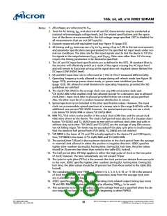
strobe are listed in Table 33 (page 62)–Table 35 (page 63) on Table 33 (page 62),
Table 34 (page 63), and Table 35 (page 63); listed values are already derated for slew
rate variations and converted from baseline values to VREF values.
31. VIL/VIH DDR2 overshoot/undershoot. See AC Overshoot/Undershoot Specification
(page 53).
32. For each input signal—not the group collectively.
33. There are two sets of values listed for command/address: tISa, tIHa and tISb, tIHb. The tISa,
tIHa values (for reference only) are equivalent to the baseline values of tISb, tIHb at VREF
when the slew rate is 1 V/ns. The baseline values, tISb, tIHb, are the JEDEC-defined values,
referenced from the logic trip points. tISb is referenced from VIH(AC) for a rising signal
and VIL(AC) for a falling signal, while tIHb is referenced from VIL(DC) for a rising signal and
VIH(DC) for a falling signal. If the command/address slew rate is not equal to 1 V/ns, then
the baseline values must be derated by adding the values from Table 28 (page 56) and
Table 29 (page 57).
34. This is applicable to READ cycles only. WRITE cycles generally require additional time
due to tWR during auto precharge.
35. READs and WRITEs with auto precharge are allowed to be issued before tRAS (MIN) is
satisfied because tRAS lockout feature is supported in DDR2 SDRAM.
36. When a single-bank PRECHARGE command is issued, tRP timing applies. tRPA timing ap-
plies when the PRECHARGE (ALL) command is issued, regardless of the number of banks
open. For 8-bank devices (≥1Gb), tRPA (MIN) = tRP (MIN) + tCK (AVG) (Table 11 (page 31)
lists tRP [MIN] + tCK [AVG] MIN).
37. This parameter has a two clock minimum requirement at any tCK.
38. The tFAW (MIN) parameter applies to all 8-bank DDR2 devices. No more than four bank-
ACTIVATE commands may be issued in a given tFAW (MIN) period. tRRD (MIN) restriction
still applies.
39. The minimum internal READ-to-PRECHARGE time. This is the time from which the last 4-
bit prefetch begins to when the PRECHARGE command can be issued. A 4-bit prefetch is
when the READ command internally latches the READ so that data will output CL later.
This parameter is only applicable when tRTP/(2 × tCK) > 1, such as frequencies faster than
533 MHz when tRTP = 7.5ns. If tRTP/(2 × tCK) ≤ 1, then equation AL + BL/2 applies. tRAS
(MIN) has to be satisfied as well. The DDR2 SDRAM will automatically delay the internal
PRECHARGE command until tRAS (MIN) has been satisfied.
40. tDAL = (nWR) + (tRP/tCK). Each of these terms, if not already an integer, should be roun-
ded up to the next integer. tCK refers to the application clock period; nWR refers to the
tWR parameter stored in the MR9–MR11. For example, -37E at tCK = 3.75ns with tWR
programmed to four clocks would have tDAL = 4 + (15ns/3.75ns) clocks = 4 + (4) clocks =
8 clocks.
41. The refresh period is 64ms (commercial) or 32ms (industrial and automotive). This equa-
tes to an average refresh rate of 7.8125µs (commercial) or 3.9607µs (industrial and
automotive). To ensure all rows of all banks are properly refreshed, 8192 REFRESH com-
mands must be issued every 64ms (commercial) or 32ms (industrial and automotive). The
JEDEC tRFC MAX of 70,000ns is not required as bursting of AUTO REFRESH commands is
allowed.
42. tDELAY is calculated from tIS + tCK + tIH so that CKE registration LOW is guaranteed pri-
or to CK, CK# being removed in a system RESET condition (see Reset (page 123)).
43. tISXR is equal to tIS and is used for CKE setup time during self refresh exit, as shown in
Figure 68 (page 114).
44. tCKE (MIN) of three clocks means CKE must be registered on three consecutive positive
clock edges. CKE must remain at the valid input level the entire time it takes to achieve
the three clocks of registration. Thus, after any CKE transition, CKE may not transition
from its valid level during the time period of tIS + 2 × tCK + tIH.
45. The half-clock of tAOFD’s 2.5 tCK assumes a 50/50 clock duty cycle. This half-clock value
must be derated by the amount of half-clock duty cycle error. For example, if the clock
PDF: 09005aef821ae8bf
1GbDDR2.pdf – Rev. T 02/10 EN
Micron Technology, Inc. reserves the right to change products or specifications without notice.
40
© 2004 Micron Technology, Inc. All rights reserved.

 MICRON [ MICRON TECHNOLOGY ]