1Gb: x4, x8, x16 DDR2 SDRAM
Output Electrical Characteristics and Operating Conditions
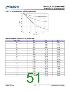
Table 19: Output Characteristics
Parameter
Min
Nom
Max
Units
Ω
Notes
1, 2
Output impedance
Pull-up and pull-down mismatch
Output slew rate
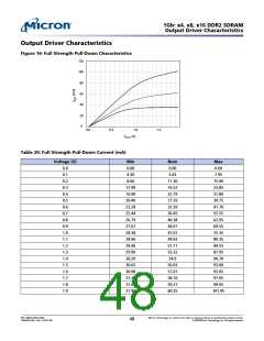
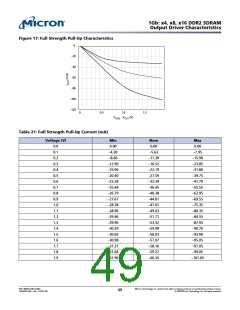
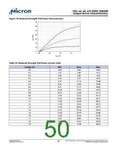
See Output Driver Characteristics (page 48)
0
4
5
1, 2, 3
1, 4, 5, 6
–
–
Ω
1.5
V/ns
1.
Notes:
Absolute specifications: 0°C ≤ TC ≤ +85°C; VDDQ = +1.8V ±0.1V, VDD = +1.8V ±0.1V.
2. Impedance measurement conditions for output source DC current: VDDQ = 1.7V;
VOUT = 1420mV; (VOUT - VDDQ)/IOH must be less than 23.4Ω for values of VOUT between
VDDQ and VDDQ - 280mV. The impedance measurement condition for output sink DC cur-
rent: VDDQ = 1.7V; VOUT = 280mV; VOUT/IOL must be less than 23.4Ω for values of VOUT
between 0V and 280mV.
3. Mismatch is an absolute value between pull-up and pull-down; both are measured at
the same temperature and voltage.
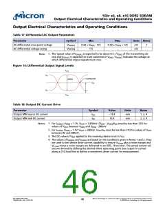
4. Output slew rate for falling and rising edges is measured between VTT - 250mV and
VTT + 250mV for single-ended signals. For differential signals (DQS, DQS#), output slew
rate is measured between DQS - DQS# = –500mV and DQS# - DQS = +500mV. Output
slew rate is guaranteed by design but is not necessarily tested on each device.
5. The absolute value of the slew rate as measured from VIL(DC)max to VIH(DC)min is equal to
or greater than the slew rate as measured from VIL(AC)max to VIH(AC)min. This is guaran-
teed by design and characterization.
6. IT and AT devices require an additional 0.4 V/ns in the MAX limit when TC is between –
40°C and 0°C.
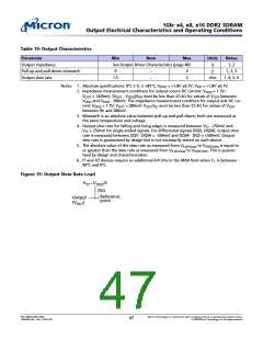
Figure 15: Output Slew Rate Load
V
= V
/2
25Ω
Reference
TT
DDQ
Output
(V
point
)
OUT
PDF: 09005aef821ae8bf
1GbDDR2.pdf – Rev. T 02/10 EN
Micron Technology, Inc. reserves the right to change products or specifications without notice.
47
© 2004 Micron Technology, Inc. All rights reserved.

 MICRON [ MICRON TECHNOLOGY ]