1Gb: x4, x8, x16 DDR2 SDRAM
AC and DC Operating Conditions
duty cycle was 47/53, tAOFD would actually be 2.5 - 0.03, or 2.47, for tAOF (MIN) and 2.5
+ 0.03, or 2.53, for tAOF (MAX).
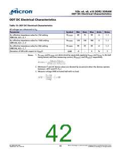
46. ODT turn-on time tAON (MIN) is when the device leaves High-Z and ODT resistance be-
gins to turn on. ODT turn-on time tAON (MAX) is when the ODT resistance is fully on.
Both are measured from tAOND.
47. ODT turn-off time tAOF (MIN) is when the device starts to turn off ODT resistance. ODT
turn off time tAOF (MAX) is when the bus is in High-Z. Both are measured from tAOFD.
48. Half-clock output parameters must be derated by the actual tERR5per and tJITdty when
input clock jitter is present; this will result in each parameter becoming larger. The pa-
rameter tAOF (MIN) is required to be derated by subtracting both tERR5per (MAX) and
tJITdty (MAX). The parameter tAOF (MAX) is required to be derated by subtracting both
tERR5per (MIN) and tJITdty (MIN).
49. The -187E maximum limit is 2 × tCK + tAC (MAX) + 1000 but it will likely be
3 x tCK + tAC (MAX) + 1000 in the future.
50. Should use 8 tCK for backward compatibility.
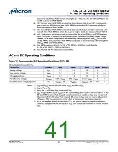
AC and DC Operating Conditions
Table 12: Recommended DC Operating Conditions (SSTL_18)
All voltages referenced to VSS
Parameter
Symbol
VDD
Min
1.7
Nom
1.8
Max
1.9
Units Notes
Supply voltage
V
V
1, 2
2, 3
2, 3
4
VDDL supply voltage
I/O supply voltage
I/O reference voltage
I/O termination voltage (system)
VDDL
1.7
1.8
1.9
VDDQ
VREF(DC)
VTT
1.7
1.8
1.9
V
0.49 × VDDQ
VREF(DC) - 40
0.50 × VDDQ
VREF(DC)
0.51 × VDDQ
VREF(DC) + 40
V
mV
5
1.
Notes:
VDD and VDDQ must track each other. VDDQ must be ≤ VDD.
2. VSSQ = VSSL = VSS.
3. VDDQ tracks with VDD; VDDL tracks with VDD
.
4. VREF is expected to equal VDDQ/2 of the transmitting device and to track variations in the
DC level of the same. Peak-to-peak noise (noncommon mode) on VREF may not exceed
±1 percent of the DC value. Peak-to-peak AC noise on VREF may not exceed ±2 percent
of VREF(DC). This measurement is to be taken at the nearest VREF bypass capacitor.
5. VTT is not applied directly to the device. VTT is a system supply for signal termination
resistors, is expected to be set equal to VREF, and must track variations in the DC level of
VREF
.
PDF: 09005aef821ae8bf
1GbDDR2.pdf – Rev. T 02/10 EN
Micron Technology, Inc. reserves the right to change products or specifications without notice.
41
© 2004 Micron Technology, Inc. All rights reserved.

 MICRON [ MICRON TECHNOLOGY ]