1Gb: x4, x8, x16 DDR2 SDRAM
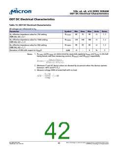
1. All voltages are referenced to VSS.
Notes:
2. Tests for AC timing, IDD, and electrical AC and DC characteristics may be conducted at
nominal reference/supply voltage levels, but the related specifications and the opera-
tion of the device are warranted for the full voltage range specified. ODT is disabled for
all measurements that are not ODT-specific.
3. Outputs measured with equivalent load (see Figure 15 (page 47)).
4. AC timing and IDD tests may use a VIL-to-VIH swing of up to 1.0V in the test environment,
and parameter specifications are guaranteed for the specified AC input levels under nor-
mal use conditions. The slew rate for the input signals used to test the device is 1.0 V/ns
for signals in the range between VIL(AC) and VIH(AC). Slew rates other than 1.0 V/ns may
require the timing parameters to be derated as specified.
5. The AC and DC input level specifications are as defined in the SSTL_18 standard (that is,
the receiver will effectively switch as a result of the signal crossing the AC input level
and will remain in that state as long as the signal does not ring back above [below] the
DC input LOW [HIGH] level).
6. CK and CK# input slew rate is referenced at 1 V/ns (2 V/ns if measured differentially).
7. Operating frequency is only allowed to change during self refresh mode (see Figure 78
(page 122)), precharge power-down mode, or system reset condition (see Reset
(page 123)). SSC allows for small deviations in operating frequency, provided the SSC
guidelines are satisfied.
8. The clock’s tCK (AVG) is the average clock over any 200 consecutive clocks and
tCK (AVG) MIN is the smallest clock rate allowed (except for a deviation due to allowed
clock jitter). Input clock jitter is allowed provided it does not exceed values specified.
Also, the jitter must be of a random Gaussian distribution in nature.
9. Spread spectrum is not included in the jitter specification values. However, the input
clock can accommodate spread spectrum at a sweep rate in the range 8–60 kHz with an
additional one percent tCK (AVG); however, the spread spectrum may not use a clock
rate below tCK (AVG) MIN or above tCK (AVG) MAX.
10. MIN (tCL, tCH) refers to the smaller of the actual clock LOW time and the actual clock
HIGH time driven to the device. The clock’s half period must also be of a Gaussian distri-
bution; tCH (AVG) and tCL (AVG) must be met with or without clock jitter and with or
without duty cycle jitter. tCH (AVG) and tCL (AVG) are the average of any 200 consecu-
tive CK falling edges. tCH limits may be exceeded if the duty cycle jitter is small enough
that the absolute half period limits (tCH [ABS], tCL [ABS]) are not violated.
11. tHP (MIN) is the lesser of tCL and tCH actually applied to the device CK and CK# inputs;
thus, tHP (MIN) ≥ the lesser of tCL (ABS) MIN and tCH (ABS) MIN.
12. The period jitter (tJITper) is the maximum deviation in the clock period from the average
or nominal clock allowed in either the positive or negative direction. JEDEC specifies
tighter jitter numbers during DLL locking time. During DLL lock time, the jitter values
should be 20 percent less those than noted in the table (DLL locked).
13. The half-period jitter (tJITdty) applies to either the high pulse of clock or the low pulse
of clock; however, the two cumulatively can not exceed tJITper.
14. The cycle-to-cycle jitter (tJITcc) is the amount the clock period can deviate from one cycle
to the next. JEDEC specifies tighter jitter numbers during DLL locking time. During DLL
lock time, the jitter values should be 20 percent less than those noted in the table (DLL
locked).
15. The cumulative jitter error (tERRnper), where n is 2, 3, 4, 5, 6–10, or 11–50 is the amount
of clock time allowed to consecutively accumulate away from the average clock over
any number of clock cycles.
16. JEDEC specifies using tERR6–10per when derating clock-related output timing (see notes
19 and 48). Micron requires less derating by allowing tERR5per to be used.
17. This parameter is not referenced to a specific voltage level but is specified when the de-
vice output is no longer driving (tRPST) or beginning to drive (tRPRE).
PDF: 09005aef821ae8bf
1GbDDR2.pdf – Rev. T 02/10 EN
Micron Technology, Inc. reserves the right to change products or specifications without notice.
38
© 2004 Micron Technology, Inc. All rights reserved.

 MICRON [ MICRON TECHNOLOGY ]