2 MEG x 16
ASYNC/PAGE/BURST FLASH MEMORY
COMMAND STATE MACHINE (CSM)
Commands are issued to the command state ma-
chine (CSM) using standard microprocessor write tim-
ings. The CSM acts as an interface between external
microprocessors and the internal write state machine
(WSM). The available commands are listed in Table 3,
their definitions are given in Table 4, and their descrip-
tions in Table 5. Program and erase algorithms are
automated by an on-chip WSM. (For more specific
information about the CSM transition states, see Micron
technical note TN-28-33, “Command State Machine De-
scription and Command Definition.”
Once a valid PROGRAM/ERASE command is entered,
the WSM executes the appropriate algorithm, which gen-
erates the necessary timing signals to control the device
internallytoaccomplishtherequestedoperation. Acom-
mand is valid only if the exact sequence of WRITEs is
completed. After the WSM completes its task, the WSM
statusbit(SR7)(seeTable7)issettoalogicꢁIGꢁlevel(1),
allowing the CSM to respond to the full command set
again.
CE#, ADV#, and OE# must be at a logic LOW level (VIL),
and WE# and RST# must be at logic ꢁIGꢁ (VIꢁ).
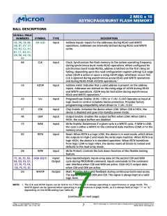
Table6illustratesthebusoperationsforallthemodes:
write, read, reset, standby, and output disable.
When the device is powered up, internal reset cir-
cuitry initializes the chip to a read array mode of opera-
tion. Changing the mode of operation requires that a
command code be entered into the CSM. For each one of
the two memory partitions, an on-chip status register is
available. These two registers allow the progress of the
various operations that can take place on a memory bank
to be monitored. One of the two status registers is inter-
rogated by entering a READ STATUS REGISTER com-
mandontotheCSM(cycle1),specifyinganaddresswithin
the memory partition boundary, and reading the register
data on I/Os DQ0–DQ7 (cycle 2). Status register bits SR0-
SR7 correspond to DQ0–DQ7 (see Table 7).
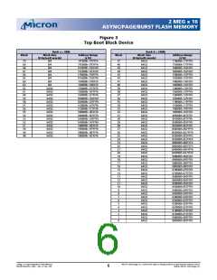
COMMAND DEFINITION
Once a specific command code has been entered, the
WSM executes an internal algorithm, generating the nec-
essary timing signals to program, erase, and verify data.
See Table 4 for the CSM command definitions and data
for each of the bus cycles.
OPERATIONS
Device operations are selected by entering a standard
JEDEC 8-bit command code with conventional micro-
processor timings into an on-chip CSM through I/Os
DQ0–DQ7. The number of bus cycles required to activate
a command is typically one or two. The first operation is
always a WRITE. Control signals CE#, ADV#, and WE#
must be at a logic LOW level (VIL), and OE# and RST#
must be at logic ꢁIGꢁ (VIꢁ). The second operation, when
needed, can be a WRITE or a READ depending upon the
command. During a READ operation, control signals
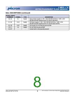
STATUS REGISTER
The status register allows the user to determine
whether the state of a PROGRAM/ERASE operation is
pending or complete. The status register is monitored by
toggling OE# and CE# and reading the resulting status
codeonI/OsDQ0–DQ7.Thehigh-orderI/Os(DQ8–DQ15)
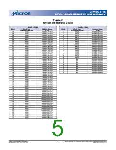
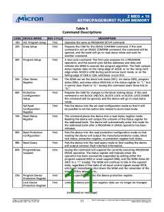
Table 3
Command State Machine Codes For Device Mode Selection
COMMAND DQ0–DQ7
CODE ON DEVICE MODE
40h/10h
20h
Program setup/alternate program setup
Block erase setup
50h
Clear status register
60h
Protection configuration setup
Set read configuration register
Read status register
60h
70h
90h
Read protection configuration register
Read query
98h
B0h
C0h
D0h
FFh
Program/erase suspend
Protection register program/lock
Program/erase resume – erase confirm
Read array
2 Meg x 16 Async/Page/Burst Flash Memory
MT28F322D20FH_4.p65 – Rev. 4, Pub. 7/02
Micron Technology, Inc., reserves the right to change products or specifications without notice.
©2002, Micron Technology, Inc.
9

 MICRON [ MICRON TECHNOLOGY ]