2 MEG x 16
ASYNC/PAGE/BURST FLASH MEMORY
DuringanERASEcycle,theCSMrespondstoanERASE
SUSPEND command only. When the WSM has com-
pleted its task, the WSM status bit (SR7) is set to a logic
ꢁIGꢁ level and the CSM responds to the full command
set. The CSM stays in the current command state until
the microprocessor issues another command.
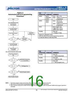
The WSM successfully initiates an ERASE or PRO-
GRAM operation only when VPP is within its correct volt-
age range.
ister, the protection register, and PR lock status. Two bus
cycles are required for this operation: the chip identifica-
tion data is read by entering the command code 90h on
DQ0–DQ7 to the bank containing address 00h and the
identification code address on the address lines. Control
signals CE#, ADV#, and OE# must be at a logic LOW level
(VIL), and WE# and RST# must be at a logic ꢁIGꢁ level
(VIꢁ) to read data from the protection configuration reg-
ister. Data is available on DQ0–DQ15. After data is read
from the protection configuration register, the READ
ARRAY command, FFh, must be issued to the bank con-
tainingaddress00hpriortoissuingothercommands. See
Table 12 for further details.
CLEAR STATUS REGISTER
The internal circuitry can set, but not clear, the block
lock status bit (SR1), the VPP status bit (SR3), the program
status bit (SR4), and the erase status bit (SR5) of the status
register. The CLEAR STATUS REGISTER command (50h)
allows the external microprocessor to clear these status
bits and synchronize to the internal operations. When
the status bits are cleared, the device returns to the read
array mode.
READ QUERY
Thereadquerymodeoutputscommonflashinterface
(CFI) data when the device is read (see Table 16). Two bus
cycles are required for this operation. It is possible to
access the query by writing the read query command
code 98h on DQ0–DQ7 to the bank containing address
0h. Control signals CE#, ADV#, and OE# must be at a logic
LOW level (VIL) and WE# and RST# must be at a logic
ꢁIGꢁlevel(VIꢁ)toreaddatafromthequery. TheCFIdata
structure contains information such as block size, den-
sity, command set, and electrical specifications. To re-
turn to read array mode, write the read array command
code FFh on DQ0–DQ7.
READ OPERATIONS
The following READ operations are available: READ
ARRAY, READ PROTECTION CONFIGURATION REGIS-
TER, READ QUERY and READ STATUS REGISTER.
READ ARRAY
The array is read by entering the command code FFh
on DQ0–DQ7. Control signals CE#, ADV#, and OE# must
be at a logic LOW level (VIL) and WE# and RST# must be
at a logic ꢁIGꢁ level (VIꢁ) to read data from the array.
Data is available on DQ0–DQ15. Any valid address within
any of the blocks selects that address and allows data to
be read from that address. Upon initial power-up or
device reset, the device defaults to the read array mode.
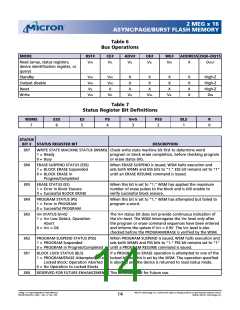
READ STATUS REGISTER
The status register is read by entering the command
code 70h on DQ0–DQ7. Two bus cycles are required for
this operation: one to enter the command code and a
second to read the status register. The address for both
cycles must be in the same partition. In a READ cycle, the
address is latched on the rising edge of the ADV# signal.
Registerdataisupdatedandlatchedonthefallingedgeof
ADV# or rising (falling) CLK when ADV# is LOW during
burst mode, or on the falling edge of OE# or CE#, which-
ever occurs last.
READ PROTECTION CONFIGURATION DATA
The read protection configuration mode outputs five
types of information: the manufacturer/device identi-
fier, the block locking status, the read configuration reg-
2 Meg x 16 Async/Page/Burst Flash Memory
MT28F322D20FH_4.p65 – Rev. 4, Pub. 7/02
Micron Technology, Inc., reserves the right to change products or specifications without notice.
13
©2002, Micron Technology, Inc.

 MICRON [ MICRON TECHNOLOGY ]