2 MEG x 16
ASYNC/PAGE/BURST FLASH MEMORY
are set to 00h internally, so only the low-order I/Os
(DQ0–DQ7) need to be interpreted. Address lines select
the status register pertinent to the selected memory
partition.
Register data is updated and latched on the falling
edge of ADV# or rising (falling) CLK when ADV# is LOW
during synchronous burst mode or on the falling edge of
OE# or CE#, whichever occurs last. Latching the data
prevents errors from occurring if the register input
changes during a status register monitoring.
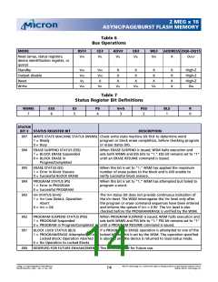
The status register provides the internal state of the
WSM to the external microprocessor. During periods
when the WSM is active, the status register can be polled
to determine the WSM status. Table 7 defines the status
register bits.
After monitoring the status register during a PRO-
GRAM/ERASE operation, the data appearing on
DQ0–DQ7 remains as status register data until a new
command is issued to the CSM. To return the device to
other modes of operation, a new command must be
issued to the CSM.
COMMAND STATE MACHINE
OPERATIONS
The CSM decodes instructions for read array, read
protection configuration register, read query, read status
register, clear status register, program, erase, erase sus-
pend, erase resume, program suspend, program resume,
lock block, unlock block and lock down block, chip pro-
tection program, and set read configuration register. The
8-bit command code is input to the device on DQ0–DQ7
(see Table 3 for CSM codes and Table 4 for command
definitions). During a PROGRAM or ERASE cycle, the
CSM informs the WSM that a PROGRAM or ERASE cycle
has been requested.
During a PROGRAM cycle, the WSM controls the pro-
gram sequences and the CSM responds to a PROGRAM
SUSPEND command only.
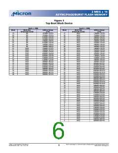
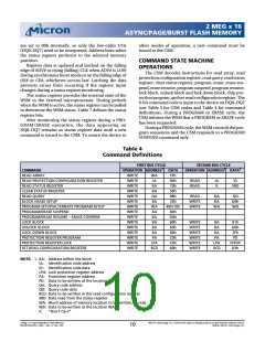
Table 4
Command Definitions
FIRST BUS CYCLE
SECOND BUS CYCLE
1
1
1
COMMAND
READ ARRAY
READ PROTECTION CONFIGURATION REGISTER
READ STATUS REGISTER
CLEAR STATUS REGISTER
READ QUERY
OPERATION ADDRESS
DATA
FFh
90h
70h
50h
98h
20h
40h/10h
B0h
D0h
60h
60h
60h
C0h
C0h
60h
OPERATION ADDRESS
DATA
WRITE
WRITE
WRITE
WRITE
WRITE
WRITE
WRITE
WRITE
WRITE
WRITE
WRITE
WRITE
WRITE
WRITE
WRITE
WA
IA
READ
READ
IA
X
ID
SRD
BA
BA
QA
BA
WA
BA
BA
BA
BA
BA
PA
READ
WRITE
WRITE
QA
BA
WA
QD
D0h
WD
BLOCK ERASE SETUP
PROGRAM SETUP/ALTERNATE PROGRAM SETUP
PROGRAM/ERASE SUSPEND
PROGRAM/ERASE RESUME – ERASE CONFIRM
LOCK BLOCK
UNLOCK BLOCK
LOCK DOWN BLOCK
PROTECTION REGISTER PROGRAM
PROTECTION REGISTER LOCK
SET READ CONFIGURATION REGISTER
WRITE
WRITE
WRITE
WRITE
WRITE
WRITE
BA
BA
BA
PA
LPA
RCD
01h
D0h
2Fh
PD
LPA
RCD
FFFDh
03h
NOTE: 1. BA: Address within the block
IA: Identification code address
ID: Identification code data
LPA: Lock protection register address
PA: Protection register address
PD: Data to be written at the location PA
QA: Query code address
QD: Query code data
RCD: Data to be written in the read configuration register
SRD: Data read from the status register
WA: Word address of memory location to be written, or read
WD: Data to be written at the location WA
X:
“Don’t Care”
2 Meg x 16 Async/Page/Burst Flash Memory
MT28F322D20FH_4.p65 – Rev. 4, Pub. 7/02
Micron Technology, Inc., reserves the right to change products or specifications without notice.
©2002, Micron Technology, Inc.
10

 MICRON [ MICRON TECHNOLOGY ]