2 MEG x 16
ASYNC/PAGE/BURST FLASH MEMORY
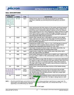
BALL DESCRIPTIONS
58-BALL FBGA
NUMBERS
SYMBOL
TYPE
DESCRIPTION
E8, D8, C8, B8,
A8, B7, A7, C7,
A2, B2, C2, A1,
B1, C1, D2, D1,
D4, B6, A6, C6,
B3
A0–A20
Input
Address Inputs: Inputs for the addresses during READ and WRITE
operations. Addresses are internally latched during READ and WRITE
cycles.
B4
CLK
Input
Clock: Synchronizes the Flash memory to the system operating frequency
during synchronous burst mode READ operations. When configured for
synchronous burst mode READs, address is latched on the first rising (or
falling, depending upon the read configuration register setting) CLK edge
when ADV# is active or upon a rising ADV# edge, whichever occurs first.
CLK is ignored during asynchronous access READ and WRITE operations
and during READ PAGE ACCESS operations.1
C4
ADV#
Input
Input
Address Valid: Indicates that a valid address is present on the address
inputs. Addresses are latched on the rising edge of ADV# during READ
and WRITE operations. ADV# may be tied active during asynchronous
READ and WRITE operations.1
A5
VPP
Program/Erase Enable: [0.9V–1.95V or 11.4V–12.6V] Operates as input at
logic levels to control complete device protection. Provides factory
programming compatibility when driven to 11.4V–12.6V.
E7
F8
C5
CE#
OE#
WE#
Input
Input
Input
Chip Enable: Activates the device when LOW. When CE# is HIGH, the
device is disabled and goes into standby power mode.
Output Enable: Enables the output buffers when LOW. When OE# is
HIGH, the output buffers are disabled.
Write Enable: Determines if a given cycle is a WRITE cycle. If WE# is LOW,
the cycle is either a WRITE to the command state machine (CSM) or to the
memory array.
B5
RST#
Input
Reset: When RST# is a logic LOW, the device is in reset mode, which drives
the outputs to High-Z and resets the write state machine. When RST# is at
logic HIGH, the device is in standard operation. When RST# transitions
from logic LOW to logic HIGH, the device resets all blocks to locked and
defaults to the read array mode.
D6
WP#
Input
Write Protect: Controls the lock down function of the flexible locking
feature.
F7, E6, E5, G5, DQ0–DQ15
E4, G3, E3, G1,
G7, F6, F5, F4,
Input/
Output
Data Inputs/Outputs: Inputs array data on the second CE# and WE#
cycle during PROGRAM command. Inputs commands to the command
user interface when CE# and WE# are active. DQ0–DQ15 output data
when CE# and OE# are active.
D5, F3, F2, E2
D3
WAIT#
Output
Wait: Provides data valid feedback during continuous burst read access.
The signal is gated by OE# and CE#. This signal is always kept at a valid
logic level.
NOTE: 1. The CLK and ADV# inputs can be tied to VSS if the device is always operating in asynchronous or page mode. The
WAIT# signal can be ignored when operating in asynchronous or page mode, as it is always held at logic “1” or “0,”
depending on the RCR8 setting (see Table 8).
(continued on next page)
2 Meg x 16 Async/Page/Burst Flash Memory
MT28F322D20FH_4.p65 – Rev. 4, Pub. 7/02
Micron Technology, Inc., reserves the right to change products or specifications without notice.
©2002, Micron Technology, Inc.
7

 MICRON [ MICRON TECHNOLOGY ]