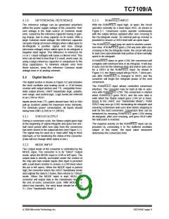
TC7109/A
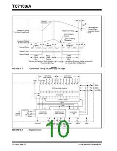
Clock
V+
23
25
24
22
÷
58
OSC
OUT
Buffered
OSC OUT
OSC OSC
SEL IN
24
22
23
25
R
OSC OSC
SEL IN
OSC
OUT
Buffered
OSC OUT
C
V+ or Open
F
OSC
= 0.45/RC
GND
Crystal
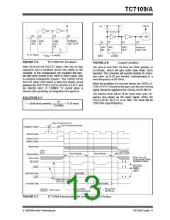
FIGURE 3-5:
TC7109A RC Oscillator
FIGURE 3-6:
Crystal Oscillator
With OSCILLATOR SELECT input LOW, two on-chip
capacitors and a feedback device are added to the
oscillator. In this configuration, the oscillator will oper-
ate with most crystals in the 1MHz to 5MHz range, with
no external components (Figure ). The OSCILLATOR
SELECT input LOW inserts a fixed 458 divider circuit
between the BUFFERED OSCILLATOR OUTPUT and
the internal clock. A 3.58MHz TV crystal gives a
division ratio, providing an integration time given by:
The error is less than 1% from two 60Hz periods, or
33.33msec, which will give better than 40dB, 60Hz
rejection. The converter will operate reliably at conver-
sion rates up to 30 per second, corresponding to a
clock frequency of 245.8kHz.
When the oscillator is to be over driven, the OSCILLA-
TOR OUTPUT should be left open, and the over driving
signal should be applied at the OSCILLATOR INPUT.
The internal clock will be of the same duty cycle, fre-
quency and phase as the input signal. When the
OSCILLATOR SELECT is at GND, the clock will be
1/58 of the input frequency.
EQUATION 3-1:
58
t = (2048 clock periods)
= 33.18 msec
3.58 MHz
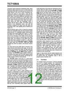
Zero Crossing Occurs
Zero Crossing Detected
Integrator Output
Internal Clock
Internal Latch
Status Output
Mode Input
UART
Norm
Terminates
UART Mode
Send Sensed
Send Sensed
Internal Mode
Mode Low, not
in Handshake Mode
Disables Outputs
Send Input
CE/LOAD
CE/LOAD,
HBEN,
HBEN
LBEN
High Byte Data
LBEN
Data Valid
Mode High Activates
CE/LOAD, HBEN, LBEN
Low Byte Data
Data Invalid
Three-State
High-Impendance
Three-State
=
=
= Don't Care
will Pull-up
FIGURE 3-7:
TC7109A Handshake with Send Input Held Positive
© 2006 Microchip Technology Inc.
DS21456C-page 13

 MICROCHIP [ MICROCHIP ]