TC7109/A
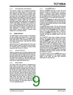
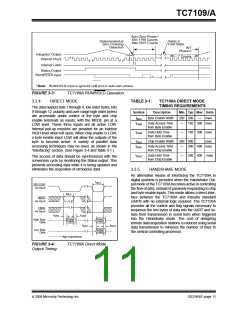
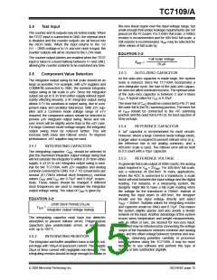
Auto-Zero Phase I
Min 1790 Counts
Max 2041 Counts
Determinated at
Zero Crossing
Detection
Static in
Hold State
INT
Phase II
Integrator Output
Internal Clock
7 Counts
Internal Latch
Status Output
RUN/HOLD Input
*
RUN/HOLD input is ignored until end of auto-zero phase.
*Note:
FIGURE 3-3:
TC7109A RUN/HOLD Operation
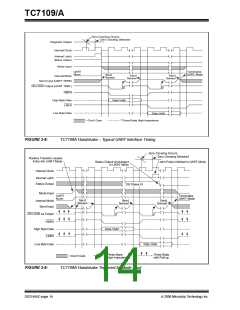
3.2.4 DIRECT MODE
TABLE 3-1:
TC7109A DIRECT MODE
TIMING REQUIREMENTS
The data outputs (bits 1 through 8, low order bytes; bits
9 through 12, polarity and over range high order bytes)
are accessible under control of the byte and chip
enable terminals as inputs, with the MODE pin at a
LOW level. These three inputs are all active LOW.
Internal pull-up resistors are provided for an inactive
HIGH level when left open. When chip enable is LOW,
a byte enable input LOW will allow the outputs of the
byte to become active. A variety of parallel data
accessing techniques may be used, as shown in the
“Interfacing” section. (See Figure 3-4 and Table 3-1.)
Symbol
Description
Min Typ Max Units
200 500 nsec
t
Byte Enable Width
—
BEA
t
Data Access Time
from Byte Enable
—
150 300 nsec
DAB
t
Data Hold Time
—
150 300 nsec
DHB
from Byte Enable
t
Chip Enable Width
300 500
nsec
CEA
t
Data Access Time
from Chip Enable
—
200 400 nsec
DAC
t
Data Hold Time
from Chip Enable
—
200 400 nsec
DHC
The access of data should be synchronized with the
conversion cycle by monitoring the Status output. This
prevents accessing data while it is being updated and
eliminates the acquisition of erroneous data.
3.2.5
HANDSHAKE MODE
An alternative means of interfacing the TC7109A to
digital systems is provided when the Handshake Out-
put mode of the TC7109A becomes active in controlling
the flow of data, instead of passively responding to chip
and byte enable inputs. This mode allows a direct inter-
face between the TC7109A and industry standard
UARTs with no external logic required. The TC7109A
provides all the control and flag signals necessary to
sequence the two bytes of data into the UART and ini-
tiate their transmission in serial form when triggered
into the Handshake mode. The cost of designing
remote data acquisition stations is reduced using serial
data transmission to minimize the number of lines to
the central controlling processor.
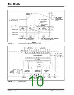
t
CEA
CE/LOAD
As Input
t
BEA
HBEN
As Input
LBEN
As Input
t
t
DAB
DAB
Data
Valid
Data
Valid
High Byte
Data
t
t
DAC
DHC
Low Byte
Data
Data
Valid
= High-Impedance
FIGURE 3-4:
TC7109A Direct Mode
Output Timing
© 2006 Microchip Technology Inc.
DS21456C-page 11

 MICROCHIP [ MICROCHIP ]