1 Mbit / 2 Mbit / 4 Mbit Multi-Purpose Flash
SST39SF010A / SST39SF020A / SST39SF040
Data Sheet
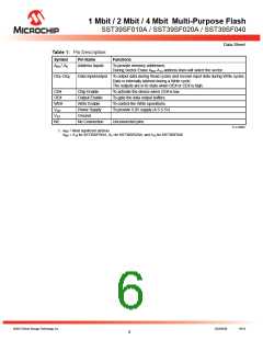
Table 1: Pin Description
Symbol
Pin Name
Functions
AMS1-A0
Address Inputs
To provide memory addresses.
During Sector-Erase AMS-A12 address lines will select the sector.
DQ7-DQ0
Data Input/output To output data during Read cycles and receive input data during Write cycles.
Data is internally latched during a Write cycle.
The outputs are in tri-state when OE# or CE# is high.
CE#
OE#
WE#
VDD
VSS
NC
Chip Enable
Output Enable
Write Enable
Power Supply
Ground
To activate the device when CE# is low.
To gate the data output buffers.
To control the Write operations.
To provide 5.0V supply (4.5-5.5V)
No Connection
Unconnected pins.
T1.2 25022
1. AMS = Most significant address
MS = A16 for SST39SF010A, A17 for SST39SF020A, and A18 for SST39SF040
A
©2013 Silicon Storage Technology, Inc.
DS25022B
04/13
6

 MICROCHIP [ MICROCHIP ]