PIC32
APPENDIX A: PIC32 FLASH
MEMORY MAP
APPENDIX B: HEX FILE FORMAT
Flash programmers process the standard hexadecimal
(hex) format used by the Microchip development tools.
The format supported is the Intel® HEX32 Format
(INHX32). Please refer to Section 1.75 “Hex file
Formats” in the “MPASM™ Assembler, MPLINK™
Object Linker, MPLIB™ Object Librarian User’s Guide”
(DS33014) for more information about hex file formats.
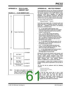
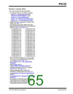
FIGURE A-1: FLASH MEMORY MAP
0x1D000000
The basic format of the hex file is:
:BBAAAATTHHHH...HHHHCC
Each data record begins with a 9-character prefix and
always ends with a 2-character checksum. All records
begin with ‘:’, regardless of the format. The individual
elements are described below.
• BB– is a two-digit hexadecimal byte count
representing the number of data bytes that appear
on the line. Divide this number by two to get the
number of words per line.
Program Flash Memory
• AAAA– is a four-digit hexadecimal address
representing the starting address of the data
record. Format is high byte first followed by low
byte. The address is doubled because this format
only supports 8 bits. Divide the value by two to
find the real device address.
• TT– is a two-digit record type that will be ‘00’ for
data records, ‘01’ for end-of-file records and ‘04’
for extended-address record.
• HHHH– is a four-digit hexadecimal data word.
Format is low byte followed by high byte. There
will be BB/2 data words following TT.
0x1D007FFF
• CC– is a two-digit hexadecimal checksum that is
the 2’s complement of the sum of all the
preceding bytes in the line record.
0x1F000000
Boot Page 0
Because the Intel hex file format is byte-oriented, and
the 16-bit program counter is not, program memory
sections require special treatment. Each 24-bit
program word is extended to 32 bits by inserting a so-
called “phantom byte”. Each program memory
address is multiplied by 2 to yield a byte address.
Boot Page 1
0x1F001FFF
Boot Page 2
Debug Page
As an example, a section that is located at 0x100 in
program memory will be represented in the hex file as
0x200.
0x1F002FF0
Configuration Words
(4 x 32 bits)
The hex file will be produced with the following
contents:
0x1F002FFF
:020000040000fa
:040200003322110096
:00000001FF
Note:
The memory map shown is for reference
only. Refer to the “Memory Organization”
chapter in the specific device data sheet for
the memory map for your device.
Notice that the data record (line 2) has a load
address of 0200, while the source code specified
address 0x100. Note also that the data is
represented in “little-endian” format, meaning the
Least Significant Byte appears first. The phantom
byte appears last, just before the checksum.
2007-2013 Microchip Technology Inc.
DS61145L-page 61

 MICROCHIP [ MICROCHIP ]