PIC32
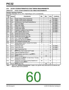
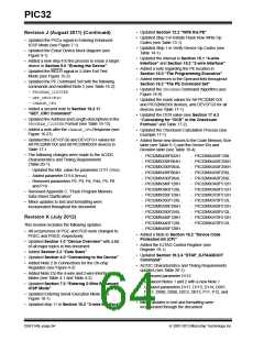
20.0 AC/DC CHARACTERISTICS AND TIMING REQUIREMENTS
TABLE 20-1: AC/DC CHARACTERISTICS AND TIMING REQUIREMENTS
Standard Operating Conditions
Operating Temperature: 0ºC to +70ºC. Programming at +25ºC is recommended.
Param.
No.
Symbol
Characteristic
Min.
Max.
Units
Conditions
D111
D113
D114
D031
D041
D080
D090
D012
D013
P1
VDD
Supply Voltage During Programming
Supply Current During Programming
Instantaneous Peak Current During Start-up
Input Low Voltage
—
—
—
—
—
—
—
—
—
—
—
—
—
—
—
—
—
—
V
mA
mA
V
See Note 1
See Note 1
See Note 1
See Note 1
See Note 1
See Note 1
See Note 1
See Note 1
See Note 1
—
IDDP
IPEAK
VIL
—
—
VIH
Input High Voltage
—
V
VOL
Output Low Voltage
—
V
VOH
Output High Voltage
—
V
CIO
Capacitive Loading on I/O pin (PGEDx)
Filter Capacitor Value on VCAP
Serial Clock (PGECx) Period
Serial Clock (PGECx) Low Time
Serial Clock (PGECx) High Time
VDD Setup Time to MCLR
Input Data Hold Time from MCLR
PE Command Processing Time
—
pF
F
ns
ns
ns
ns
ns
s
s
CF
—
TPGC
TPGCL
TPGCH
TSET2
THLD2
TDLY4
TDLY5
100
40
40
100
500
40
15
P1A
P1B
P6
—
—
—
P7
—
P9A
P9B
—
Delay between PGEDx by the PE to PGEDx
—
Released by the PE
P11
P12
P13
TDLY7
TDLY8
TDLY9
Chip Erase Time
—
—
—
—
10
0
—
—
—
ms
ms
ms
See Note 1
See Note 1
See Note 1
Page Erase Time
Row Programming Time
P14
P15
P16
TR
MCLR Rise Time to Enter ICSP™ mode
Data Out Valid from PGECx
1.0
—
s
ns
s
—
—
—
TVALID
TDLY8
Delay between Last PGECx and MCLR
—
P17
P18
THLD3
TKEY1
MCLR to VDD
—
100
—
ns
ns
—
—
Delay from First MCLR to First PGECx for Key
40
Sequence on PGEDx
P19
TKEY2
Delay from Last PGECx for Key Sequence on
PGEDx to Second MCLR
40
—
ns
—
P20
TMCLRH MCLR High Time
—
500
µs
—
Note 1: Refer to the “Electrical Characteristics” chapter in the specific device data sheet for the Minimum and
Maximum values for this parameter.
DS61145L-page 60
2007-2013 Microchip Technology Inc.

 MICROCHIP [ MICROCHIP ]