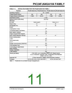
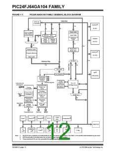
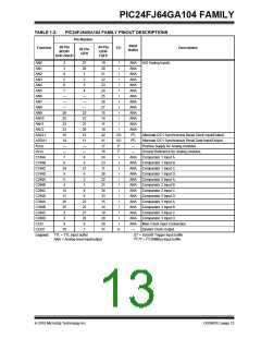
PIC24FJ64GA104 FAMILY
• Instruction-Based Power-Saving Modes: There
are three instruction-based power-saving modes:
1.0
DEVICE OVERVIEW
This document contains device-specific information for
the following devices:
- Idle Mode – The core is shut down while leaving
the peripherals active.
• PIC24FJ32GA102
• PIC24FJ64GA102
• PIC24FJ32GA104
• PIC24FJ64GA104
- Sleep Mode – The core and peripherals that
require the system clock are shut down, leaving
the peripherals active that use their own clock or
the clock from other devices.
The PIC24FJ64GA104 family provides an expanded
peripheral feature set and new option for
high-performance applications which may need more
than an 8-bit platform, but do not require the power of a
digital signal processor.
a
- Deep Sleep Mode – The core, peripherals
(except RTCC and DSWDT), Flash and SRAM
are shut down for optimal current savings to
extend battery life for portable applications.
1.1
Core Features
1.1.3
OSCILLATOR OPTIONS AND
FEATURES
1.1.1
16-BIT ARCHITECTURE
All of the devices in the PIC24FJ64GA104 family offer
five different oscillator options, allowing users a range
of choices in developing application hardware. These
include:
Central to all PIC24F devices is the 16-bit modified
Harvard architecture, first introduced with Microchip’s
dsPIC® digital signal controllers. The PIC24F CPU core
offers a wide range of enhancements, such as:
• Two Crystal modes using crystals or ceramic
resonators.
• 16-bit data and 24-bit address paths with the
ability to move information between data and
memory spaces
• Two External Clock modes offering the option of a
divide-by-2 clock output.
• Linear addressing of up to 12 Mbytes (program
space) and 64 Kbytes (data)
• A Fast Internal Oscillator (FRC) with a nominal
8 MHz output, which can also be divided under
software control to provide clock speeds as low as
31 kHz.
• A 16-element working register array with built-in
software stack support
• A 17 x 17 hardware multiplier with support for
integer math
• A Phase Lock Loop (PLL) frequency multiplier
available to the external oscillator modes and the
FRC Oscillator, which allows clock speeds of up
to 32 MHz.
• Hardware support for 32 by 16-bit division
• An instruction set that supports multiple
addressing modes and is optimized for high-level
languages, such as ‘C’
• A separate Low-Power Internal RC Oscillator
(LPRC) with a fixed 31 kHz output, which pro-
vides a low-power option for timing-insensitive
applications.
• Operational performance up to 16 MIPS
1.1.2
POWER-SAVING TECHNOLOGY
The internal oscillator block also provides a stable
reference source for the Fail-Safe Clock Monitor. This
option constantly monitors the main clock source
against a reference signal provided by the internal
oscillator and enables the controller to switch to the
internal oscillator, allowing for continued low-speed
operation or a safe application shutdown.
All of the devices in the PIC24FJ64GA104 family
incorporate a range of features that can significantly
reduce power consumption during operation. Key
items include:
• On-the-Fly Clock Switching: The device clock
can be changed under software control to the
Timer1 source or the internal, Low-Power Internal
RC Oscillator during operation, allowing the user
to incorporate power-saving ideas into their
software designs.
1.1.4
EASY MIGRATION
Regardless of the memory size, all devices share the
same rich set of peripherals, allowing for a smooth
migration path as applications grow and evolve. The
consistent pinout scheme used throughout the entire
family also aids in migrating from one device to the next
larger device.
• Doze Mode Operation: When timing-sensitive
applications, such as serial communications,
require the uninterrupted operation of peripherals,
the CPU clock speed can be selectively reduced,
allowing incremental power savings without
missing a beat.
The PIC24F family is pin-compatible with devices in the
dsPIC33 family, and shares some compatibility with the
pinout schema for PIC18 and dsPIC30 devices. This
extends the ability of applications to grow from the
relatively simple, to the powerful and complex, yet still
selecting a Microchip device.
2010 Microchip Technology Inc.
DS39951C-page 9

 MICROCHIP [ MICROCHIP ]