PIC24FJ64GA104 FAMILY
1.2
Other Special Features
1.3
Details on Individual Family
Members
• Peripheral Pin Select: The Peripheral Pin Select
feature allows most digital peripherals to be
mapped over a fixed set of digital I/O pins. Users
may independently map the input and/or output of
any one of the many digital peripherals to any one
of the I/O pins.
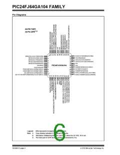
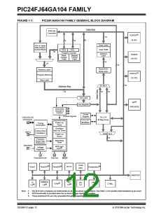
Devices in the PIC24FJ64GA104 family are available
in 28-pin and 44-pin packages. The general block
diagram for all devices is shown in Figure 1-1.
The devices are differentiated from each other in
several ways:
• Communications: The PIC24FJ64GA104 family
incorporates a range of serial communication
peripherals to handle a range of application
requirements. There are two independent I2C™
modules that support both Master and Slave
modes of operation. Devices also have, through
the Peripheral Pin Select (PPS) feature, two
independent UARTs with built-in IrDA®
• Flash Program Memory:
- PIC24FJ32GA1 devices – 32 Kbytes
- PIC24FJ64GA1 devices – 64 Kbytes
• Available I/O Pins and Ports:
- 28-pin devices – 21 pins on two ports
- 44-pin devices – 35 pins on three ports
• Available Interrupt-on-Change Notification (ICN)
Inputs:
encoder/decoders and two SPI modules.
• Analog Features: All members of the
- 28-pin devices – 21
PIC24FJ64GA104 family include a 10-bit A/D
Converter module and a triple comparator
module. The A/D module incorporates program-
mable acquisition time, allowing for a channel to
be selected and a conversion to be initiated
without waiting for a sampling period, as well as
faster sampling speeds. The comparator module
includes three analog comparators that are
configurable for a wide range of operations.
- 44-pin devices – 31
• Available Remappable Pins:
- 28-pin devices – 16 pins
- 44-pin devices – 26 pins
• Available PMP Address Pins:
- 28-pin devices – 3 pins
- 44-pin devices – 12 pins
• Available A/D Input Channels:
- 28-pin devices – 10 pins
- 44-pin devices – 13 pins
• CTMU Interface: This module provides a
convenient method for precision time measure-
ment and pulse generation, and can serve as an
interface for capacitive sensors.
All other features for devices in this family are identical.
These are summarized in Table 1-1.
• Parallel Master/Enhanced Parallel Slave Port:
One of the general purpose I/O ports can be
reconfigured for enhanced parallel data communi-
cations. In this mode, the port can be configured
for both master and slave operations, and
A
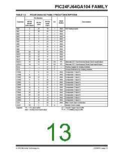
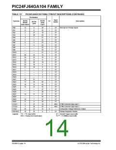
list of the pin features available on the
PIC24FJ64GA104 family devices, sorted by function, is
shown in Table 1-2. Note that this table shows the pin
location of individual peripheral features and not how
they are multiplexed on the same pin. This information
is provided in the pinout diagrams in the beginning of
this data sheet. Multiplexed features are sorted by the
priority given to a feature, with the highest priority
peripheral being listed first.
supports 8-bit and 16-bit data transfers with up to
12 external address lines in Master modes.
• Real-Time Clock/Calendar: This module
implements a full-featured clock and calendar with
alarm functions in hardware, freeing up timer
resources and program memory space for the use
of the core application.
DS39951C-page 10
2010 Microchip Technology Inc.

 MICROCHIP [ MICROCHIP ]