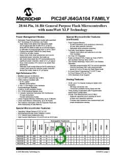
PIC24FJ64GA104 FAMILY
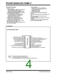
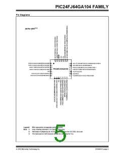
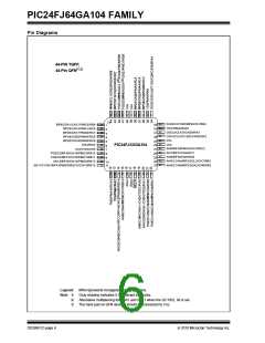
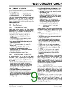
Pin Diagrams
28-Pin QFN(1,3)
28 27 26 25 24 2322
PGED1/AN2/C2INB/RP0/CN4/RB0
AN11/C1INC/RP13/CN13/PMRD/REFO/RB13
1
2
3
4
5
6
7
21
PGEC1/AN3/C2INA/RP1/CN5/RB1
AN4/C1INB/SDA2/RP2/CN6/RB2
AN12/RP12/CN14/PMD0/RB12
20
PGEC2/TMS/RP11/CN15/PMD1/RB11
19
PIC24FJXXGA102
AN5/C1INA/SCL2/RP3/CN7/RB3
PGED2/TDI/RP10/CN16/PMD2/RB10
18
VSS
VCAP/VDDCORE
17
OSCI/CLKI/C1IND/CN30/RA2
OSCO/CLKO/CN29/PMA0/RA3
DISVREG
16
15
TDO/RP9/SDA1/CN21/PMD3/RB9
8
9 10 11 12 13 14
Legend:
RPn represents remappable peripheral pins.
Note 1: Gray shading indicates 5.5V tolerant input pins.
2: Alternative multiplexing for SDA1 and SCL1 when the I2C1SEL bit is set.
3: The back pad on QFN devices should be connected to VSS.
2010 Microchip Technology Inc.
DS39951C-page 5

 MICROCHIP [ MICROCHIP ]