PIC24FJ64GA104 FAMILY
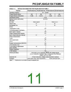
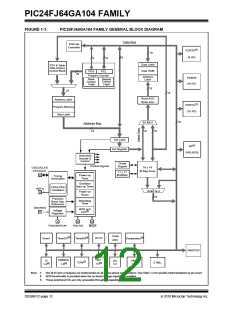
FIGURE 1-1:
PIC24FJ64GA104 FAMILY GENERAL BLOCK DIAGRAM
Data Bus
Interrupt
Controller
PORTA(1)
(9 I/O)
16
16
16
8
Data Latch
Data RAM
PSV & Table
Data Access
Control Block
PCH
PCL
23
Program Counter
Address
Latch
PORTB
(16 I/O)
Stack
Control
Logic
Repeat
Control
Logic
16
23
16
Read AGU
Write AGU
Address Latch
Program Memory
Data Latch
PORTC(1)
(10 I/O)
16
EA MUX
Address Bus
24
16
16
Inst Latch
RP(1)
Inst Register
RP0:RP25
Instruction
Decode &
Control
Divide
Support
Control Signals
16 x 16
W Reg Array
OSCO/CLKO
OSCI/CLKI
17 x 17
Multiplier
Power-up
Timer
Timing
Generation
Oscillator
Start-up Timer
FRC/LPRC
Oscillators
REFO
16-Bit ALU
Power-on
Reset
16
Precision
Band Gap
Reference
Watchdog
Timer
DISVREG
BOR and
LVD(2)
Voltage
Regulator
VDDCORE/VCAP
VDD,VSS
MCLR
10-Bit
Timer2/3(3)
Comparators(3)
Timer4/5(3)
RTCC
Timer1
ADC
PMP/PSP
PWM/OC
1-5(3)
SPI
1/2(3)
IC
1-5(3)
UART
1/2(3)
I2C
1/2
ICNs(1)
CTMU
Note 1: Not all I/O pins or features are implemented on all device pinout configurations. See Table 1-2 for specific implementations by pin count
.
2: BOR functionality is provided when the on-board voltage regulator is enabled.
3: These peripheral I/Os are only accessible through remappable pins.
DS39951C-page 12
2010 Microchip Technology Inc.

 MICROCHIP [ MICROCHIP ]