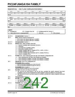
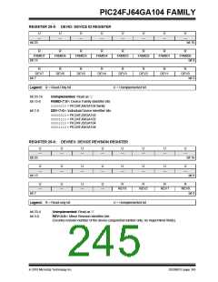
PIC24FJ64GA104 FAMILY
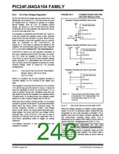
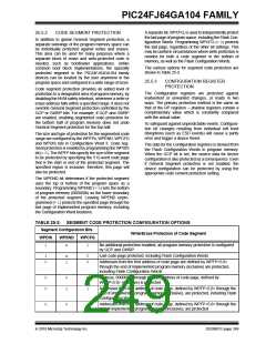
FIGURE 25-1:
CONNECTIONS FOR THE
ON-CHIP REGULATOR
25.2 On-Chip Voltage Regulator
All PIC24FJ64GA104 family devices power their core
digital logic at a nominal 2.5V. This may create an issue
for designs that are required to operate at a higher
typical voltage, such as 3.3V. To simplify system
design, all devices in the PIC24FJ64GA104 family
incorporate an on-chip regulator that allows the device
to run its core logic from VDD.
Regulator Enabled (DISVREG tied to VSS):
3.3V
PIC24FJ64GA104
VDD
DISVREG
VDDCORE/VCAP
CEFC
(10 F typ)
The regulator is controlled by the DISVREG pin. Tying VSS
to the pin enables the regulator, which in turn, provides
power to the core from the other VDD pins. When the reg-
ulator is enabled, a low-ESR capacitor (such as ceramic)
VSS
must be connected to the
VDDCORE/VCAP pin
(Figure 25-1). This helps to maintain the stability of the
regulator. The recommended value for the Filter Capacitor
Regulator Disabled (DISVREG tied to VDD):
(1)
(1)
2.5V
3.3V
(CEFC) is provided in Section 28.1 “DC Characteristics”
.
PIC24FJ64GA104
If DISVREG is tied to VDD, the regulator is disabled. In
this case, separate power for the core logic, at a nomi-
nal 2.5V, must be supplied to the device on the
VDDCORE/VCAP pin to run the I/O pins at higher voltage
levels, typically 3.3V. Alternatively, the VDDCORE/VCAP
and VDD pins can be tied together to operate at a lower
nominal voltage. Refer to Figure 25-1 for possible
configurations.
VDD
DISVREG
VDDCORE/VCAP
VSS
Regulator Disabled (VDD tied to VDDCORE):
25.2.1
VOLTAGE REGULATOR TRACKING
MODE AND LOW-VOLTAGE
DETECTION
(1)
2.5V
PIC24FJ64GA104
VDD
When it is enabled, the on-chip regulator provides a
constant voltage of 2.5V nominal to the digital core
logic.
DISVREG
VDDCORE/VCAP
VSS
The regulator can provide this level from a VDD of about
2.5V, all the way up to the device’s VDDMAX. It does not
have the capability to boost VDD levels below 2.5V. In
order to prevent “brown-out” conditions when the volt-
age drops too low for the regulator, the regulator enters
Tracking mode. In Tracking mode, the regulator output
follows VDD with a typical voltage drop of 100 mV.
Note 1: These are typical operating voltages. Refer
to Section 28.1 “DC Characteristics” for
the full operating ranges of VDD and
VDDCORE.
When the device enters Tracking mode, it is no longer
possible to operate at full speed. To provide information
about when the device enters Tracking mode, the
on-chip regulator includes a simple, Low-Voltage
Detect circuit. When VDD drops below full-speed oper-
ating voltage, the circuit sets the Low-Voltage Detect
Interrupt Flag, LVDIF (IFS4<8>). This can be used to
generate an interrupt and put the application into a
Low-Power Operational mode or trigger an orderly
shutdown.
25.2.2
ON-CHIP REGULATOR AND POR
When the voltage regulator is enabled, it takes approxi-
mately 10 s for it to generate output. During this time,
designated as TPM, code execution is disabled. TPM is
applied every time the device resumes operation after
any power-down, including Sleep mode. TPM is
determined by the setting of the PMSLP bit (RCON<8>)
and the WUTSEL Configuration bits (CW3<11:10>).
Low-Voltage Detection is only available when the
regulator is enabled.
Note:
For more information on TPM, see
Section 28.0 “Electrical Characteristics”.
If the regulator is disabled, a separate Power-up Timer
(PWRT) is automatically enabled. The PWRT adds a
fixed delay of 64 ms nominal delay at device start-up
(POR or BOR only).
DS39951C-page 246
2010 Microchip Technology Inc.

 MICROCHIP [ MICROCHIP ]