PIC24FJ64GA104 FAMILY
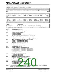
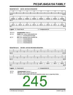
REGISTER 25-2: CW2: FLASH CONFIGURATION WORD 2
U-1
—
U-1
—
U-1
—
U-1
—
U-1
—
U-1
—
U-1
—
U-1
—
bit 23
bit 16
R/PO-1
IESO
U-1
—
U-1
—
U-1
—
U-1
—
R/PO-1
R/PO-1
R/PO-1
FNOSC2
FNOSC1
FNOSC0
bit 15
bit 8
R/PO-1
R/PO-1
R/PO-1
R/PO-1
U-1
—
R/PO-1
R/PO-1
R/PO-1
FCKSM1
FCKSM0
OSCIOFCN
IOL1WAY
I2C1SEL
POSCMD1
POSCMD0
bit 7
bit 0
Legend:
R = Readable bit
PO = Program Once bit
U = Unimplemented bit, read as ‘0’
‘1’ = Bit is set ‘0’ = Bit is cleared
-n = Value when device is unprogrammed
bit 23-16
bit 15
Unimplemented: Read as ‘1’
IESO: Internal External Switchover bit
1= IESO mode (Two-Speed Start-up) is enabled
0= IESO mode (Two-Speed Start-up) is disabled
bit 14-11
bit 10-8
Unimplemented: Read as ‘1’
FNOSC<2:0>: Initial Oscillator Select bits
111= Fast RC Oscillator with Postscaler (FRCDIV)
110= Reserved
101= Low-Power RC Oscillator (LPRC)
100= Secondary Oscillator (SOSC)
011= Primary Oscillator with PLL module (XTPLL, HSPLL, ECPLL)
010= Primary Oscillator (XT, HS, EC)
001= Fast RC Oscillator with Postscaler and PLL module (FRCPLL)
000= Fast RC Oscillator (FRC)
bit 7-6
bit 5
FCKSM<1:0>: Clock Switching and Fail-Safe Clock Monitor Configuration bits
1x= Clock switching and Fail-Safe Clock Monitor are disabled
01= Clock switching is enabled, Fail-Safe Clock Monitor is disabled
00= Clock switching is enabled, Fail-Safe Clock Monitor is enabled
OSCIOFCN: OSCO Pin Configuration bit
If POSCMD<1:0> = 11 or 00:
1= OSCO/CLKO/RA3 functions as CLKO (FOSC/2)
0= OSCO/CLKO/RA3 functions as port I/O (RC15)
If POSCMD<1:0> = 10 or 01:
OSCIOFCN has no effect on OSCO/CLKO/RA3.
bit 4
IOL1WAY: IOLOCK One-Way Set Enable bit
1= The IOLOCK bit (OSCCON<6>) can be set once, provided the unlock sequence has been
completed. Once set, the Peripheral Pin Select registers cannot be written to a second time.
0= The IOLOCK bit can be set and cleared as needed, provided the unlock sequence has been
completed
bit 3
bit 2
Unimplemented: Read as ‘1’
I2C1SEL: I2C1 Pin Select bit
1= Use default SCL1/SDA1 pins
0= Use alternate SCL1/SDA1 pins
bit 1-0
POSCMD<1:0>: Primary Oscillator Configuration bits
11= Primary Oscillator is disabled
10= HS Oscillator mode is selected
01= XT Oscillator mode is selected
00= EC Oscillator mode is selected
DS39951C-page 242
2010 Microchip Technology Inc.

 MICROCHIP [ MICROCHIP ]