PIC24FJ64GA104 FAMILY
When waking up from Sleep with the regulator
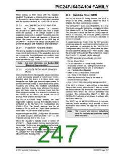
25.3 Watchdog Timer (WDT)
disabled, TPM is used to determine the wake-up time.
To decrease the device wake-up time when operating
with the regulator disabled, the PMSLP bit can be set.
For PIC24FJ64GA104 family devices, the WDT is
driven by the LPRC Oscillator. When the WDT is
enabled, the clock source is also enabled.
25.2.3
When
ON-CHIP REGULATOR AND BOR
the on-chip regulator is enabled,
The nominal WDT clock source from LPRC is 31 kHz.
This feeds a prescaler that can be configured for either
5-bit (divide-by-32) or 7-bit (divide-by-128) operation.
The prescaler is set by the FWPSA Configuration bit.
With a 31 kHz input, the prescaler yields a nominal
WDT time-out period (TWDT) of 1 ms in 5-bit mode, or
4 ms in 7-bit mode.
PIC24FJ64GA104 family devices also have a simple
brown-out capability. If the voltage supplied to the
regulator is inadequate to maintain the tracking level, the
regulator Reset circuitry will generate a Brown-out
Reset. This event is captured by the BOR flag bit
(RCON<1>). The brown-out voltage specifications are
provided in Section 28.0 “Electrical Characteristics”.
A variable postscaler divides down the WDT prescaler
output and allows for a wide range of time-out periods.
The postscaler is controlled by the WDTPS<3:0>
Configuration bits (CW1<3:0>), which allow the selec-
tion of a total of 16 settings, from 1:1 to 1:32,768. Using
the prescaler and postscaler time-out periods, ranges
from 1 ms to 131 seconds can be achieved.
25.2.4
POWER-UP REQUIREMENTS
The on-chip regulator is designed to meet the power-up
requirements for the device. If the application does not
use the regulator, then strict power-up conditions must
be adhered to. While powering up, VDDCORE must
never exceed VDD by 0.3 volts.
The WDT, prescaler and postscaler are reset:
• On any device Reset
Note:
For more information, see Section 28.0
“Electrical Characteristics”.
• On the completion of a clock switch, whether
invoked by software (i.e., setting the OSWEN bit
after changing the NOSC bits) or by hardware
(i.e., Fail-Safe Clock Monitor)
25.2.5
VOLTAGE REGULATOR STANDBY
MODE
• When a PWRSAVinstruction is executed
When enabled, the on-chip regulator always consumes
a small incremental amount of current over IDD/IPD,
including when the device is in Sleep mode, even
though the core digital logic does not require power. To
provide additional savings in applications where power
resources are critical, the regulator automatically
places itself into Standby mode whenever the device
goes into Sleep mode by removing power from the
Flash program memory. This feature is controlled by
the PMSLP bit (RCON<8>). By default, this bit is
cleared, which enables Standby mode.
(i.e., Sleep or Idle mode is entered)
• When the device exits Sleep or Idle mode to
resume normal operation
• By a CLRWDTinstruction during normal execution
If the WDT is enabled, it will continue to run during
Sleep or Idle modes. When the WDT time-out occurs,
the device will wake the device and code execution will
continue from where the PWRSAV instruction was
executed. The corresponding SLEEP or IDLE bits
(RCON<3:2>) will need to be cleared in software after
the device wakes up.
For PIC24FJ64GA104 family devices, the time
required for regulator wake-up from Standby mode is
controlled by the WUTSEL<1:0> Configuration bits
(CW3<11:10>). The default wake-up time for all
devices is 190 s, which is a Legacy mode provided to
match older PIC24F device wake-up times.
The WDT Flag bit, WDTO (RCON<4>), is not auto-
matically cleared following a WDT time-out. To detect
subsequent WDT events, the flag must be cleared in
software.
Note:
The CLRWDT and PWRSAV instructions
clear the prescaler and postscaler counts
when executed.
Implementing the WUTSEL Configuration bits provides
a fast wake-up option. When WUTSEL<1:0> = 01, the
regulator wake-up time is TPM, 10 s.
When the regulator’s Standby mode is turned off
(PMSLP = 1), Flash program memory stays powered in
Sleep mode. That enables device wake-up without wait-
ing for TPM. With PMSLP set, however, the power
consumption, while in Sleep mode, will be approximately
40 A higher than what it would be if the regulator was
allowed to enter Standby mode.
2010 Microchip Technology Inc.
DS39951C-page 247

 MICROCHIP [ MICROCHIP ]