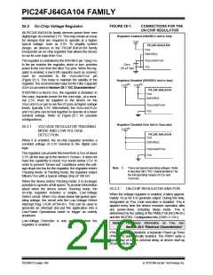
PIC24FJ64GA104 FAMILY
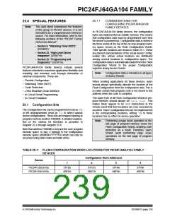
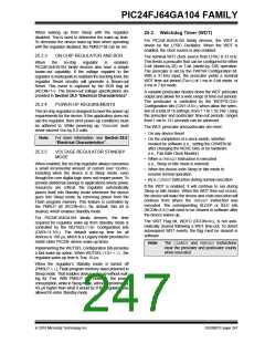
REGISTER 25-3: CW3: FLASH CONFIGURATION WORD 3
U-1
—
U-1
—
U-1
—
U-1
—
U-1
—
U-1
—
U-1
—
U-1
—
bit 23
bit 16
R/PO-1
R/PO-1
R/PO-1
WPDIS
U-1
—
R/PO-1
R/PO-1
R/PO-1
R/PO-1
WPEND
WPCFG
WUTSEL1
WUTSEL0
SOSCSEL1(1) SOSCSEL0(1)
bit 15
bit 8
U-1
—
U-1
—
R/PO-1
WPFP5
R/PO-1
WPFP4
R/PO-1
WPFP3
R/PO-1
WPFP2
R/PO-1
WPFP1
R/PO-1
WPFP0
bit 7
bit 0
Legend:
R = Readable bit
PO = Program Once bit
U = Unimplemented bit, read as ‘0’
‘1’ = Bit is set ‘0’ = Bit is cleared
-n = Value when device is unprogrammed
bit 23-16
bit 15
Unimplemented: Read as ‘1’
WPEND: Segment Write Protection End Page Select bit
1= Protected code segment lower boundary is at the bottom of program memory (000000h); upper
boundary is the code page specified by WPFP<8:0>
0= Protected code segment upper boundary is at the last page of program memory; lower boundary
is the code page specified by WPFP<8:0>
bit 14
bit 13
WPCFG: Configuration Word Code Page Protection Select bit
1= Last page (at the top of program memory) and Flash Configuration Words are not protected
0= Last page and Flash Configuration Words are code-protected
WPDIS: Segment Write Protection Disable bit
1= Segmented code protection is disabled
0= Segmented code protection is enabled; protected segment defined by WPEND, WPCFG and
WPFPx Configuration bits
bit 12
Unimplemented: Read as ‘1’
bit 11-10
WUTSEL<1:0>: Voltage Regulator Standby Mode Wake-up Time Select bits
11= Default regulator start-up time used
01= Fast regulator start-up time used
x0= Reserved; do not use
bit 9-8
SOSCSEL<1:0>: Secondary Oscillator Power Mode Select bits(1)
11= SOSC pins are in default (high drive strength) oscillator mode
01= SOSC pins are in Low-Power (low drive strength) Oscillator mode
00= SOSC pins have digital I/O functions (RA4, RB4); SCLKI can be used
10= Reserved
bit 7-6
bit 5-0
Unimplemented: Read as ‘1’
WPFP5:WPFP0: Protected Code Segment Boundary Page bits
Designates the 512 instruction page that is the boundary of the protected code segment, starting with
Page 9 at the bottom of program memory.
If WPEND = 1:
Last address of designated code page is the upper boundary of the segment.
If WPEND = 0:
First address of designated code page is the lower boundary of the segment.
Note 1: Digital functions on the SOSCI and SOSCO pins are only available when configured in Digital I/O mode
(‘00’).
2010 Microchip Technology Inc.
DS39951C-page 243

 MICROCHIP [ MICROCHIP ]