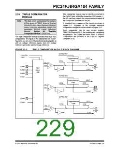
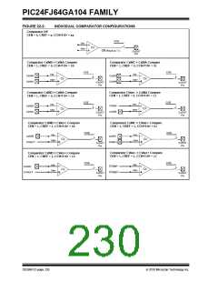
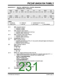
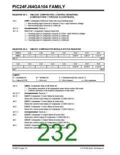
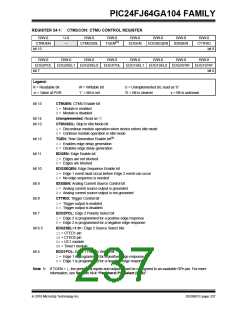
PIC24FJ64GA104 FAMILY
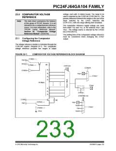
voltage, each with 16 distinct levels. The range to be
used is selected by the CVRR bit (CVRCON<5>). The
primary difference between the ranges is the size of the
steps selected by the CVREF Selection bits
23.0 COMPARATOR VOLTAGE
REFERENCE
Note:
This data sheet summarizes the features
(CVR<3:0>), with one range offering finer resolution.
of this group of PIC24F devices. It is not
intended to be a comprehensive reference
source. For more information, refer to the
“PIC24F Family Reference Manual”,
Section 20. “Comparator Voltage
Reference Module” (DS39709).
The comparator reference supply voltage can come
from either VDD and VSS, or the external VREF+ and
VREF-. The voltage source is selected by the CVRSS
bit (CVRCON<4>).
The settling time of the comparator voltage reference
must be considered when changing the CVREF
output.
23.1 Configuring the Comparator
Voltage Reference
The voltage reference module is controlled through the
CVRCON register (Register 23-1). The comparator
voltage reference provides two ranges of output
FIGURE 23-1:
COMPARATOR VOLTAGE REFERENCE BLOCK DIAGRAM
CVRSS = 1
CVRSS = 0
VREF+
AVDD
8R
CVR<3:0>
CVREFP
R
CVREN
1
R
R
R
VREF+
CVREF+
0
16 Steps
CVREF
R
R
R
CVROE
CVREFM<1:0>
CVRR
VREF-
8R
CVRSS = 1
VREF+
VBG/6
11
10
CVREF-
CVRSS = 0
01
00
VBG
AVSS
VBG/2
2010 Microchip Technology Inc.
DS39951C-page 233

 MICROCHIP [ MICROCHIP ]