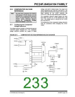
PIC24FJ64GA104 FAMILY
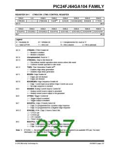
When the module is configured for pulse generation
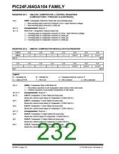
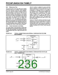
24.2 Measuring Time
delay by setting the TGEN bit (CTMUCON<12>), the
internal current source is connected to the B input of
Comparator 2. A capacitor (CDELAY) is connected to
the Comparator 2 pin, C2INB, and the comparator volt-
age reference, CVREF, is connected to C2INA. CVREF
is then configured for a specific trip point. The module
begins to charge CDELAY when an edge event is
detected. When CDELAY charges above the CVREF trip
point, a pulse is output on CTPLS. The length of the
pulse delay is determined by the value of CDELAY and
the CVREF trip point.
Time measurements on the pulse width can be similarly
performed using the A/D module’s internal capacitor
(CAD) and a precision resistor for current calibration.
Figure 24-2 shows the external connections used for
time measurements, and how the CTMU and A/D
modules are related in this application. This example
also shows both edge events coming from the external
CTEDG pins, but other configurations using internal
edge sources are possible. For the smallest time
measurements, select the internal A/D Channel 31,
CH0Sx <4:0>= 11111. This minimizes any stray capac-
itance that may otherwise be associated with using an
input pin, thus keeping the total capacitance to that of the
A/D Converter itself (4-5 pF). A detailed discussion on
measuring capacitance and time with the CTMU module
is provided in the “PIC24F Family Reference Manual”.
Figure 24-3 shows the external connections for pulse
generation, as well as the relationship of the different
analog modules required. While CTEDG1 is shown as
the input pulse source, other options are available. A
detailed discussion on pulse generation with the CTMU
module is provided in the “PIC24F Family Reference
Manual”.
24.3 Pulse Generation and Delay
The CTMU module can also generate an output pulse
with edges that are not synchronous with the device’s sys-
tem clock. More specifically, it can generate a pulse with
a programmable delay from an edge event input to the
module.
FIGURE 24-2:
TYPICAL CONNECTIONS AND INTERNAL CONFIGURATION FOR TIME
MEASUREMENT
PIC24F Device
CTMU
CTEDG1
CTEDG2
EDG1
EDG2
Current Source
Output
Pulse
A/D Converter
ANx
RPR
CAD
FIGURE 24-3:
TYPICAL CONNECTIONS AND INTERNAL CONFIGURATION FOR PULSE
DELAY GENERATION
PIC24F Device
CTMU
CTEDG1
EDG1
CTPLS
Current Source
Comparator
C2
C2INB
CDELAY
CVREF
DS39951C-page 236
2010 Microchip Technology Inc.

 MICROCHIP [ MICROCHIP ]