PIC24FJ64GA104 FAMILY
The comparator outputs may be directly connected to
the CxOUT pins. When the respective COE equals ‘1’,
the I/O pad logic makes the unsynchronized output of
the comparator available on the pin.
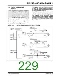
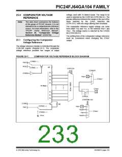
22.0 TRIPLE COMPARATOR
MODULE
Note:
This data sheet summarizes the features
of this group of PIC24F devices. It is not
A simplified block diagram of the module in shown in
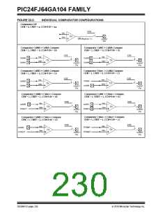
Figure 22-1. Diagrams of the possible individual
comparator configurations are shown in Figure 22-2.
intended to be a comprehensive reference
source. For more information, refer to the
associated “PIC24F Family Reference
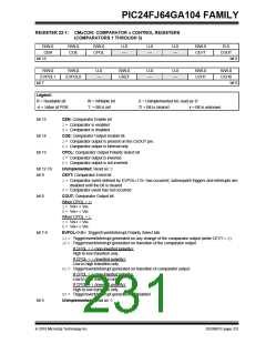
Each comparator has its own control register,
CMxCON (Register 22-1), for enabling and configuring
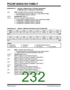
its operation. The output and event status of all three
comparators are provided in the CMSTAT register
(Register 22-2).
Manual”,
Section
46.
“Scalable
Comparator Module” (DS39734)
The triple comparator module provides three dual input
comparators. The inputs to the comparator can be con-
figured to use any one of four external analog inputs, as
well as voltage reference inputs from the voltage
reference generator and band gap reference.
FIGURE 22-1:
TRIPLE COMPARATOR MODULE BLOCK DIAGRAM
EVPOL<1:0>
CCH<1:0>
CREF
CEVT
Trigger/Interrupt
Logic
COE
CPOL
VIN-
C1
VIN+
CXINB
CXINC
CXIND
CVREF-
C1OUT
Pin
Input
Select
Logic
COUT
CEVT
EVPOL<1:0>
CPOL
Trigger/Interrupt
Logic
COE
VIN-
C2
VIN+
C2OUT
Pin
COUT
CEVT
EVPOL<1:0>
CPOL
CXINA
Trigger/Interrupt
Logic
CVREF+
COE
VIN-
C3
VIN+
C3OUT
Pin
COUT
2010 Microchip Technology Inc.
DS39951C-page 229

 MICROCHIP [ MICROCHIP ]