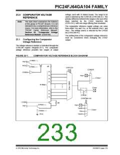
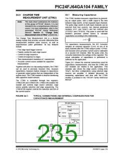
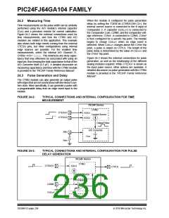
PIC24FJ64GA104 FAMILY
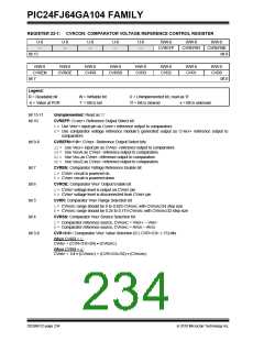
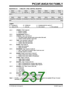
REGISTER 24-1: CTMUCON: CTMU CONTROL REGISTER
R/W-0
U-0
—
R/W-0
R/W-0
TGEN(1)
R/W-0
R/W-0
R/W-0
R/W-0
CTMUEN
CTMUSIDL
EDGEN
EDGSEQEN
IDISSEN
CTTRIG
bit 15
bit 8
R/W-0
R/W-0
R/W-0
R/W-0
R/W-0
R/W-0
R/W-0
R/W-0
EDG2POL
EDG2SEL1 EDG2SEL0
EDG1POL
EDG1SEL1 EDG1SEL0 EDG2STAT EDG1STAT
bit 0
bit 7
Legend:
R = Readable bit
-n = Value at POR
W = Writable bit
‘1’ = Bit is set
U = Unimplemented bit, read as ‘0’
‘0’ = Bit is cleared
x = Bit is unknown
bit 15
CTMUEN: CTMU Enable bit
1= Module is enabled
0= Module is disabled
bit 14
bit 13
Unimplemented: Read as ‘0’
CTMUSIDL: Stop in Idle Mode bit
1= Discontinue module operation when device enters Idle mode
0= Continue module operation in Idle mode
bit 12
bit 11
bit 10
bit 9
TGEN: Time Generation Enable bit(1)
1= Enables edge delay generation
0= Disables edge delay generation
EDGEN: Edge Enable bit
1= Edges are not blocked
0= Edges are blocked
EDGSEQEN: Edge Sequence Enable bit
1= Edge 1 event must occur before Edge 2 event can occur
0= No edge sequence is needed
IDISSEN: Analog Current Source Control bit
1= Analog current source output is grounded
0= Analog current source output is not grounded
bit 8
CTTRIG: Trigger Control bit
1= Trigger output is enabled
0= Trigger output is disabled
bit 7
EDG2POL: Edge 2 Polarity Select bit
1= Edge 2 is programmed for a positive edge response
0= Edge 2 is programmed for a negative edge response
bit 6-5
EDG2SEL<1:0>: Edge 2 Source Select bits
11= CTED1 pin
10= CTED2 pin
01= OC1 module
00= Timer1 module
bit 4
EDG1POL: Edge 1 Polarity Select bit
1= Edge 1 is programmed for a positive edge response
0= Edge 1 is programmed for a negative edge response
Note 1: If TGEN = 1, the peripheral inputs and outputs must be configured to an available RPn pin. For more
information, see Section 10.4 “Peripheral Pin Select (PPS)”.
2010 Microchip Technology Inc.
DS39951C-page 237

 MICROCHIP [ MICROCHIP ]