PIC24FJ64GA104 FAMILY
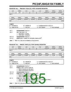
REGISTER 18-2: PMMODE: PARALLEL PORT MODE REGISTER
R-0
R/W-0
R/W-0
R/W-0
R/W-0
R/W-0
R/W-0
R/W-0
BUSY
IRQM1
IRQM0
INCM1
INCM0
MODE16
MODE1
MODE0
bit 15
bit 8
R/W-0
R/W-0
R/W-0
R/W-0
R/W-0
R/W-0
R/W-0
R/W-0
WAITB1(1)
WAITB0(1)
WAITM3
WAITM2
WAITM1
WAITM0
WAITE1(1)
WAITE0(1)
bit 7
bit 0
Legend:
R = Readable bit
-n = Value at POR
W = Writable bit
‘1’ = Bit is set
U = Unimplemented bit, read as ‘0’
‘0’ = Bit is cleared x = Bit is unknown
bit 15
BUSY: Busy bit (Master mode only)
1= Port is busy (not useful when the processor stall is active)
0= Port is not busy
bit 14-13
IRQM<1:0>: Interrupt Request Mode bits
11= Interrupt generated when Read Buffer 3 is read or Write Buffer 3 is written (Buffered PSP mode),
or on a read or write operation when PMA<1:0> = 11(Addressable PSP mode only)
10= No interrupt is generated, processor stall activated
01= Interrupt is generated at the end of the read/write cycle
00= No interrupt is generated
bit 12-11
INCM<1:0>: Increment Mode bits
11= PSP read and write buffers auto-increment (Legacy PSP mode only)
10= Decrement ADDR<10:0> by 1 every read/write cycle
01= Increment ADDR<10:0> by 1 every read/write cycle
00= No increment or decrement of address
bit 10
MODE16: 8/16-Bit Mode bit
1= 16-bit mode: Data register is 16 bits; a read or write to the Data register invokes two 8-bit transfers
0= 8-bit mode: Data register is 8 bits; a read or write to the Data register invokes one 8-bit transfer
bit 9-8
MODE<1:0>: Parallel Port Mode Select bits
11= Master Mode 1 (PMCS1, PMRD/PMWR, PMENB, PMBE, PMA<x:0> and PMD<7:0>)
10= Master Mode 2 (PMCS1, PMRD, PMWR, PMBE, PMA<x:0> and PMD<7:0>)
01= Enhanced PSP control signals (PMRD, PMWR, PMCS1, PMD<7:0> and PMA<1:0>)
00= Legacy Parallel Slave Port control signals (PMRD, PMWR, PMCS1 and PMD<7:0>)
bit 7-6
bit 5-2
bit 1-0
WAITB<1:0>: Data Setup to Read/Write Wait State Configuration bits(1)
11= Data wait of 4 TCY; multiplexed address phase of 4 TCY
10= Data wait of 3 TCY; multiplexed address phase of 3 TCY
01= Data wait of 2 TCY; multiplexed address phase of 2 TCY
00= Data wait of 1 TCY; multiplexed address phase of 1 TCY
WAITM<3:0>: Read to Byte Enable Strobe Wait State Configuration bits
1111= Wait of additional 15 TCY
...
0001= Wait of additional 1 TCY
0000= No additional wait cycles (operation forced into one TCY)
WAITE<1:0>: Data Hold After Strobe Wait State Configuration bits(1)
11= Wait of 4 TCY
10= Wait of 3 TCY
01= Wait of 2 TCY
00= Wait of 1 TCY
Note 1: WAITB and WAITE bits are ignored whenever WAITM<3:0> = 0000.
DS39951C-page 194
2010 Microchip Technology Inc.

 MICROCHIP [ MICROCHIP ]