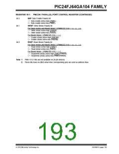
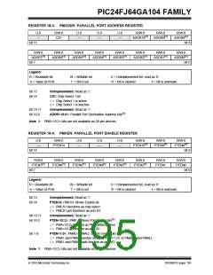
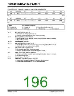
PIC24FJ64GA104 FAMILY
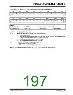
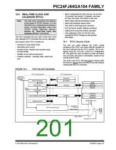
REGISTER 18-6: PADCFG1: PAD CONFIGURATION CONTROL REGISTER
U-0
—
U-0
—
U-0
—
U-0
—
U-0
—
U-0
—
U-0
—
U-0
—
bit 15
bit 8
U-0
—
U-0
—
U-0
—
U-0
—
U-0
—
R/W-0
R/W-0
R/W-0
(1)
(1)
RTSECSEL1
RTSECSEL0
PMPTTL
bit 7
bit 0
Legend:
R = Readable bit
-n = Value at POR
W = Writable bit
‘1’ = Bit is set
U = Unimplemented bit, read as ‘0’
‘0’ = Bit is cleared x = Bit is unknown
bit 15-3
bit 2-1
Unimplemented: Read as ‘0’
RTSECSEL<1:0>: RTCC Seconds Clock Output Select bits(1)
11= Reserved; do not use
10= RTCC source clock is selected for the RTCC pin (clock can be LPRC or SOSC, depending on the
setting of the Flash Configuration bit, RTCOSC (CW4<5>))
01= RTCC seconds clock is selected for the RTCC pin
00= RTCC alarm pulse is selected for the RTCC pin
bit 0
PMPTTL: PMP Module TTL Input Buffer Select bit
1= PMP module uses TTL input buffers
0= PMP module uses Schmitt Trigger input buffers
Note 1: To enable the actual RTCC output, the RTCOE (RCFGCAL<10>) bit needs to be set.
2010 Microchip Technology Inc.
DS39951C-page 197

 MICROCHIP [ MICROCHIP ]