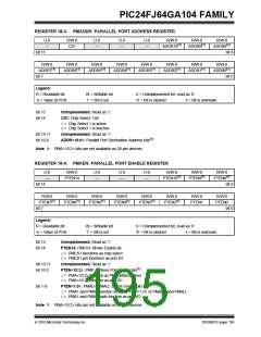
PIC24FJ64GA104 FAMILY
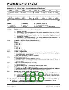
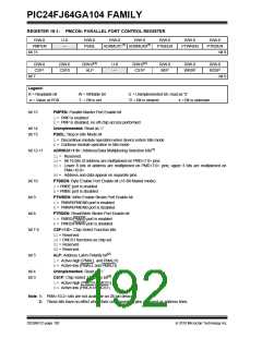
REGISTER 18-1: PMCON: PARALLEL PORT CONTROL REGISTER
R/W-0
U-0
—
R/W-0
PSIDL
R/W-0
R/W-0
R/W-0
R/W-0
R/W-0
(1)
(1)
PMPEN
ADRMUX1
ADRMUX0
PTBEEN
PTWREN
PTRDEN
bit 15
bit 8
R/W-0
CSF1
R/W-0
CSF0
R/W-0(2)
ALP
U-0
—
R/W-0(2)
CS1P
R/W-0
BEP
R/W-0
WRSP
R/W-0
RDSP
bit 7
bit 0
Legend:
R = Readable bit
-n = Value at POR
W = Writable bit
‘1’ = Bit is set
U = Unimplemented bit, read as ‘0’
‘0’ = Bit is cleared x = Bit is unknown
bit 15
PMPEN: Parallel Master Port Enable bit
1= PMP is enabled
0= PMP is disabled, no off-chip access performed
bit 14
bit 13
Unimplemented: Read as ‘0’
PSIDL: Stop in Idle Mode bit
1= Discontinue module operation when device enters Idle mode
0= Continue module operation in Idle mode
bit 12-11
ADRMUX<1:0>: Address/Data Multiplexing Selection bits(1)
11= Reserved
10= All 16 bits of address are multiplexed on PMD<7:0> pins
01= Lower 8 bits of address are multiplexed on PMD<7:0> pins; upper 3 bits are multiplexed on
PMA<10:8>
00= Address and data appear on separate pins
bit 10
bit 9
PTBEEN: Byte Enable Port Enable bit (16-Bit Master mode)
1= PMBE port is enabled
0= PMBE port is disabled
PTWREN: Write Enable Strobe Port Enable bit
1= PMWR/PMENB port is enabled
0= PMWR/PMENB port is disabled
bit 8
PTRDEN: Read/Write Strobe Port Enable bit
1= PMRD/PMWR port is enabled
0= PMRD/PMWR port is disabled
bit 7-6
CSF<1:0>: Chip Select Function bits
11= Reserved
10= PMCS1 functions as chip set
01= Reserved
00= Reserved
bit 5
ALP: Address Latch Polarity bit(2)
1= Active-high (PMALL and PMALH)
0= Active-low (PMALL and PMALH)
bit 4
bit 3
Unimplemented: Read as ‘0’
CS1P: Chip Select 1 Polarity bit(2)
1= Active-high (PMCS1/PMCS1)
0= Active-low (PMCS1/PMCS1)
Note 1: PMA<10:2> bits are not available on 28-pin devices.
2: These bits have no effect when their corresponding pins are used as address lines.
DS39951C-page 192
2010 Microchip Technology Inc.

 MICROCHIP [ MICROCHIP ]