PIC24FJ64GA104 FAMILY
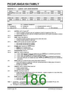
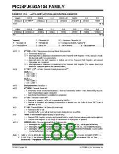
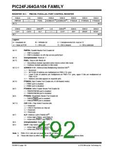
REGISTER 17-2: UxSTA: UARTx STATUS AND CONTROL REGISTER
R/W-0
UTXISEL1
bit 15
R/W-0
UTXINV(1)
R/W-0
U-0
—
R/W-0, HC
UTXBRK
R/W-0
UTXEN(2)
R-0
R-1
UTXISEL0
UTXBF
TRMT
bit 8
R/W-0
URXISEL1
bit 7
R/W-0
R/W-0
R-1
R-0
R-0
R/C-0
R-0
URXISEL0
ADDEN
RIDLE
PERR
FERR
OERR
URXDA
bit 0
Legend:
C = Clearable bit
W = Writable bit
‘1’ = Bit is set
HC = Hardware Clearable bit
U = Unimplemented bit, read as ‘0’
‘0’ = Bit is cleared x = Bit is unknown
R = Readable bit
-n = Value at POR
bit 15,13
UTXISEL<1:0>: Transmission Interrupt Mode Selection bits
11= Reserved; do not use
10= Interrupt when a character is transferred to the Transmit Shift Register (TSR), and as a result,
the transmit buffer becomes empty
01= Interrupt when the last character is shifted out of the Transmit Shift Register; all transmit
operations are completed
00= Interrupt when a character is transferred to the Transmit Shift Register (this implies there is at
least one character open in the transmit buffer)
bit 14
UTXINV: IrDA® Encoder Transmit Polarity Inversion bit(1)
IREN = 0:
1= UxTX Idle ‘0’
0= UxTX Idle ‘1’
IREN = 1:
1= UxTX Idle ‘1’
0= UxTX Idle ‘0’
bit 12
bit 11
Unimplemented: Read as ‘0’
UTXBRK: Transmit Break bit
1= Send Sync Break on next transmission – Start bit, followed by twelve ‘0’ bits, followed by Stop bit;
cleared by hardware upon completion
0= Sync Break transmission is disabled or completed
bit 10
UTXEN: Transmit Enable bit(2)
1= Transmit is enabled, UxTX pin is controlled by UARTx
0= Transmit is disabled, any pending transmission is aborted and the buffer is reset; UxTX pin is
controlled by port
bit 9
UTXBF: Transmit Buffer Full Status bit (read-only)
1= Transmit buffer is full
0= Transmit buffer is not full; at least one more character can be written
bit 8
TRMT: Transmit Shift Register Empty bit (read-only)
1= Transmit Shift Register is empty and transmit buffer is empty (the last transmission has completed)
0= Transmit Shift Register is not empty, a transmission is in progress or queued
bit 7-6
URXISEL<1:0>: Receive Interrupt Mode Selection bits
11= Interrupt is set on RSR transfer, making the receive buffer full (i.e., has 4 data characters)
10= Interrupt is set on RSR transfer, making the receive buffer 3/4 full (i.e., has 3 data characters)
0x= Interrupt is set when any character is received and transferred from the RSR to the receive buffer;
receive buffer has one or more characters
Note 1: Value of bit only affects the transmit properties of the module when the IrDA encoder is enabled (IREN = 1).
2: If UARTEN = 1, the peripheral inputs and outputs must be configured to an available RPn pin. See
Section 10.4 “Peripheral Pin Select (PPS)” for more information.
DS39951C-page 188
2010 Microchip Technology Inc.

 MICROCHIP [ MICROCHIP ]