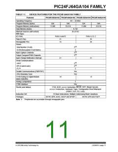
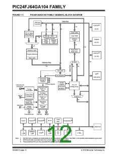
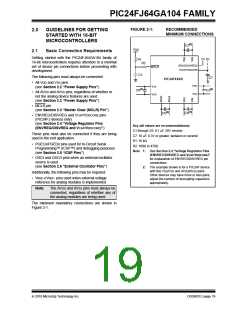
PIC24FJ64GA104 FAMILY
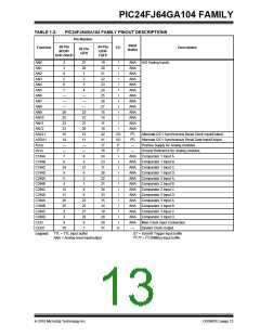
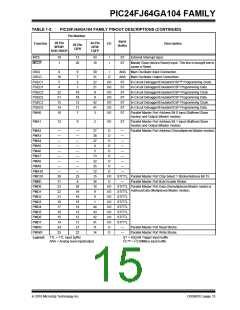
TABLE 1-2:
PIC24FJ64GA104 FAMILY PINOUT DESCRIPTIONS (CONTINUED)
Pin Number
Input
Buffer
28-Pin
SPDIP/
SOIC/SSOP
44-Pin
QFN/
TQFP
Function
I/O
Description
28-Pin
QFN
INT0
16
1
13
26
43
18
I
I
ST
ST
External Interrupt Input.
MCLR
Master Clear (device Reset) Input. This line is brought low to
cause a Reset.
OSCI
9
6
7
30
31
22
21
9
I
ANA
ANA
ST
Main Oscillator Input Connection.
OSCO
PGEC1
PGED1
PGEC2
PGED2
PGEC3
PGED3
PMA0
10
5
O
Main Oscillator Output Connection.
2
I/O
I/O
I/O
I/O
I/O
I/O
I/O
In-Circuit Debugger/Emulator/ICSP™ Programming Clock.
In-Circuit Debugger/Emulator/ICSP Programming Data.
In-Circuit Debugger/Emulator/ICSP Programming Clock.
In-Circuit Debugger/Emulator/ICSP Programming Data.
In-Circuit Debugger/Emulator/ICSP Programming Clock.
In-Circuit Debugger/Emulator/ICSP Programming Data.
4
1
ST
22
21
15
14
10
19
18
12
11
7
ST
8
ST
42
41
3
ST
ST
ST
Parallel Master Port Address Bit 0 Input (Buffered Slave
modes) and Output (Master modes).
PMA1
12
9
2
I/O
ST
Parallel Master Port Address Bit 1 Input (Buffered Slave
modes) and Output (Master modes).
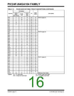
PMA2
PMA3
PMA4
PMA5
PMA6
PMA7
PMA8
PMA9
PMA10
PMCS1
PMBE
PMD0
PMD1
PMD2
PMD3
PMD4
PMD5
PMD6
PMD7
PMRD
PMWR
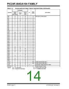
Legend:
—
—
—
—
—
—
—
—
—
26
11
23
22
21
18
17
16
15
14
24
25
—
—
—
—
—
—
—
—
—
23
8
27
38
37
4
O
O
—
—
—
—
—
—
—
—
—
Parallel Master Port Address (Demultiplexed Master modes).
O
O
5
O
13
32
35
12
15
36
10
9
O
O
O
O
I/O
O
ST/TTL Parallel Master Port Chip Select 1 Strobe/Address Bit 15.
Parallel Master Port Byte Enable Strobe.
—
20
19
18
15
14
13
12
11
21
22
I/O
I/O
I/O
I/O
I/O
I/O
I/O
I/O
O
ST/TTL Parallel Master Port Data (Demultiplexed Master mode) or
Address/Data (Multiplexed Master modes).
ST/TTL
8
ST/TTL
ST/TTL
ST/TTL
ST/TTL
ST/TTL
ST/TTL
1
44
43
42
41
11
14
—
—
Parallel Master Port Read Strobe.
Parallel Master Port Write Strobe.
O
TTL = TTL input buffer
ANA = Analog level input/output
ST = Schmitt Trigger input buffer
2
2
I C™ = I C/SMBus input buffer
2010 Microchip Technology Inc.
DS39951C-page 15

 MICROCHIP [ MICROCHIP ]