PIC18F2480/2580/4480/4580
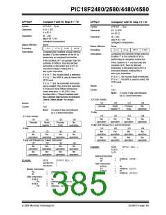
CPFSEQ
Compare f with W, Skip if f = W
COMF
Complement f
Syntax:
CPFSEQ f {,a}
Syntax:
COMF f {,d {,a}}
Operands:
0 ≤ f ≤ 255
a ∈ [0,1]
Operands:
0 ≤ f ≤ 255
d ∈ [0,1]
a ∈ [0,1]
Operation:
(f) – (W),
skip if (f) = (W)
(unsigned comparison)
Operation:
(f) → dest
Status Affected:
Encoding:
N, Z
Status Affected:
Encoding:
None
0001
11da
ffff
ffff
0110
001a
ffff
ffff
Description:
The contents of register ‘f’ are
Description:
Compares the contents of data memory
location ‘f’ to the contents of W by
performing an unsigned subtraction.
complemented. If ‘d’ is ‘1’, the result is
stored in W. If ‘d’ is ‘0’, the result is
stored back in register ‘f’.
If ‘f’ = W, then the fetched instruction is
discarded and a NOPis executed
instead, making this a two-cycle
instruction.
If ‘a’ is ‘0’, the Access Bank is selected.
If ‘a’ is ‘1’, the BSR is used to select the
GPR bank.
If ‘a’ is ‘0’ and the extended instruction
set is enabled, this instruction operates
in Indexed Literal Offset Addressing
mode whenever f ≤ 95 (5Fh). See
Section 26.2.3 “Byte-Oriented and
Bit-Oriented Instructions in Indexed
Literal Offset Mode” for details.
If ‘a’ is ‘0’, the Access Bank is selected.
If ‘a’ is ‘0’, the BSR is used to select the
GPR bank.
If ‘a’ is ‘0’ and the extended instruction
set is enabled, this instruction operates
in Indexed Literal Offset Addressing
mode whenever f ≤ 95 (5Fh). See
Section 26.2.3 “Byte-Oriented and
Bit-Oriented Instructions in Indexed
Literal Offset Mode” for details.
Words:
Cycles:
1
1
Q Cycle Activity:
Q1
Words:
Cycles:
1
Q2
Q3
Q4
1(2)
Decode
Read
register ‘f’
Process
Data
Write to
destination
Note: 3 cycles if skip and followed
by a 2-word instruction.
Q Cycle Activity:
Q1
Example:
COMF
REG, 0, 0
Q2
Read
register ‘f’
Q3
Process
Data
Q4
No
operation
Before Instruction
Decode
REG
=
13h
After Instruction
If skip:
REG
W
=
=
13h
ECh
Q1
No
Q2
No
Q3
No
Q4
No
operation
operation
operation
operation
If skip and followed by 2-word instruction:
Q1
No
Q2
No
Q3
No
Q4
No
operation
No
operation
No
operation
No
operation
No
operation
operation
operation
operation
Example:
HERE
CPFSEQ REG, 0
NEQUAL
EQUAL
:
:
Before Instruction
PC Address
=
=
=
HERE
?
?
W
REG
After Instruction
If REG
PC
If REG
PC
=
=
≠
=
W;
Address (EQUAL)
W;
Address (NEQUAL)
DS39637D-page 384
© 2009 Microchip Technology Inc.

 MICROCHIP [ MICROCHIP ]