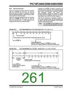
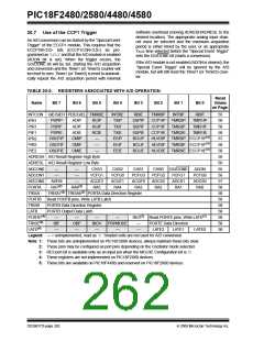
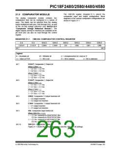
PIC18F2480/2580/4480/4580
21.3.2
INTERNAL REFERENCE SIGNAL
21.2 Comparator Operation
The comparator module also allows the selection of an
internally generated voltage reference from the com-
parator voltage reference module. This module is
described in more detail in Section 22.0 “Comparator
Voltage Reference Module”.
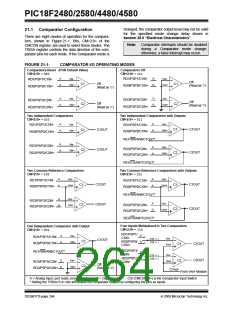
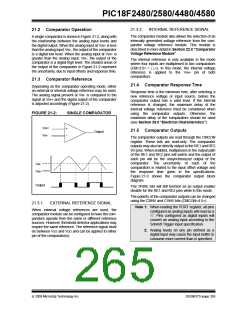
A single comparator is shown in Figure 21-2, along with
the relationship between the analog input levels and
the digital output. When the analog input at VIN+ is less
than the analog input VIN-, the output of the comparator
is a digital low level. When the analog input at VIN+ is
greater than the analog input, VIN-, the output of the
comparator is a digital high level. The shaded areas of
the output of the comparator in Figure 21-2 represent
the uncertainty, due to input offsets and response time.
The internal reference is only available in the mode
where four inputs are multiplexed to two comparators
(CM<2:0> = 110). In this mode, the internal voltage
reference is applied to the VIN+ pin of both
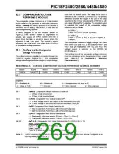
comparators.
21.3 Comparator Reference
21.4 Comparator Response Time
Depending on the comparator operating mode, either
an external or internal voltage reference may be used.
The analog signal present at VIN- is compared to the
signal at VIN+ and the digital output of the comparator
is adjusted accordingly (Figure 21-2).
Response time is the minimum time, after selecting a
new reference voltage or input source, before the
comparator output has a valid level. If the internal
reference is changed, the maximum delay of the
internal voltage reference must be considered when
using the comparator outputs. Otherwise, the
maximum delay of the comparators should be used
(see Section 28.0 “Electrical Characteristics”).
FIGURE 21-2:
SINGLE COMPARATOR
VIN+
VIN-
+
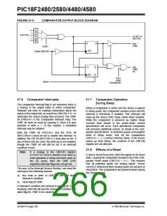
21.5 Comparator Outputs
Output
–
The comparator outputs are read through the CMCON
register. These bits are read-only. The comparator
outputs may also be directly output to the RE1 and RE2
I/O pins. When enabled, multiplexers in the output path
of the RE1 and RE2 pins will switch and the output of
each pin will be the unsynchronized output of the
comparator. The uncertainty of each of the
comparators is related to the input offset voltage and
the response time given in the specifications.
Figure 21-3 shows the comparator output block
diagram.
VIN-
VIN+
Output
The TRISE bits will still function as an output enable/
disable for the RE1 and RE2 pins while in this mode.
The polarity of the comparator outputs can be changed
using the C2INV and C1INV bits (CMCON<4:5>).
21.3.1
EXTERNAL REFERENCE SIGNAL
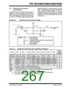
Note 1: When reading the PORT register, all pins
configured as analog inputs will read as a
‘0’. Pins configured as digital inputs will
convert an analog input according to the
Schmitt Trigger input specification.
When external voltage references are used, the
comparator module can be configured to have the com-
parators operate from the same or different reference
sources. However, threshold detector applications may
require the same reference. The reference signal must
be between VSS and VDD and can be applied to either
pin of the comparator(s).
2: Analog levels on any pin defined as a
digital input may cause the input buffer to
consume more current than is specified.
© 2009 Microchip Technology Inc.
DS39637D-page 265

 MICROCHIP [ MICROCHIP ]