PIC18F2480/2580/4480/4580
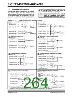
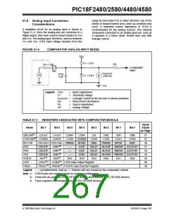
The CMCON register (Register 21-1) selects the
comparator input and output configuration. Block
diagrams of the various comparator configurations are
shown in Figure 21-1.
21.0 COMPARATOR MODULE
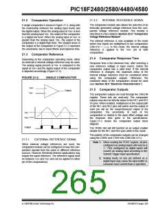
The analog comparator module contains two
comparators that can be configured in a variety of
ways. The inputs can be selected from the analog
inputs multiplexed with pins, RA0 through RA5, as well
as the on-chip voltage reference (see Section 22.0
“Comparator Voltage Reference Module”). The
digital outputs (normal or inverted) are available at the
pin level and can also be read through the control
register.
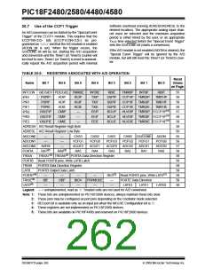
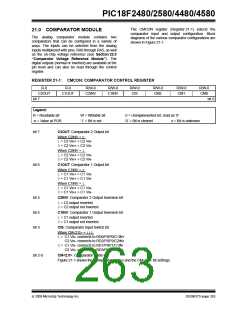
REGISTER 21-1: CMCON: COMPARATOR CONTROL REGISTER
R-0
R-0
R/W-0
C2INV
R/W-0
C1INV
R/W-0
CIS
R/W-0
CM2
R/W-0
CM1
R/W-0
CM0
C2OUT
C1OUT
bit 7
bit 0
Legend:
R = Readable bit
-n = Value at POR
W = Writable bit
‘1’ = Bit is set
U = Unimplemented bit, read as ‘0’
‘0’ = Bit is cleared x = Bit is unknown
bit 7
C2OUT: Comparator 2 Output bit
When C2INV = 0:
1= C2 VIN+ > C2 VIN-
0= C2 VIN+ < C2 VIN-
When C2INV = 1:
1= C2 VIN+ < C2 VIN-
0= C2 VIN+ > C2 VIN-
bit 6
C1OUT: Comparator 1 Output bit
When C1INV = 0:
1= C1 VIN+ > C1 VIN-
0= C1 VIN+ < C1 VIN-
When C1INV = 1:
1= C1 VIN+ < C1 VIN-
0= C1 VIN+ > C1 VIN-
bit 5
bit 4
bit 3
C2INV: Comparator 2 Output Inversion bit
1= C2 output inverted
0= C2 output not inverted
C1INV: Comparator 1 Output Inversion bit
1= C1 output inverted
0= C1 output not inverted
CIS: Comparator Input Switch bit
When CM<2:0> = 110:
1= C1 VIN- connects to RD0/PSP0/C1IN+
C2 VIN- connects to RD2/PSP2/C2IN+
0= C1 VIN- connects to RD1/PSP1/C1IN-
C2 VIN- connects to RD3/PSP3/C2IN-
bit 2-0
CM<2:0>: Comparator Mode bits
Figure 21-1 shows the Comparator modes and the CM<2:0> bit settings.
© 2009 Microchip Technology Inc.
DS39637D-page 263

 MICROCHIP [ MICROCHIP ]