PIC18F2480/2580/4480/4580
software overhead (moving ADRESH/ADRESL to the
20.7 Use of the CCP1 Trigger
desired location). The appropriate analog input chan-
nel must be selected and the minimum acquisition
period is either timed by the user, or an appropriate
TACQ time selected before the “Special Event Trigger”
sets the GO/DONE bit (starts a conversion).
An A/D conversion can be started by the “Special Event
Trigger” of the ECCP1 module. This requires that the
ECCP1M<3:0> bits (ECCP1CON<3:0>) be pro-
grammed as ‘1011’ and that the A/D module is enabled
(ADON bit is set). When the trigger occurs, the
GO/DONE bit will be set, starting the A/D acquisition
and conversion and the Timer1 (or Timer3) counter will
be reset to zero. Timer1 (or Timer3) is reset to automat-
ically repeat the A/D acquisition period with minimal
If the A/D module is not enabled (ADON is cleared), the
“Special Event Trigger” will be ignored by the A/D
module, but will still reset the Timer1 (or Timer3) coun-
ter.
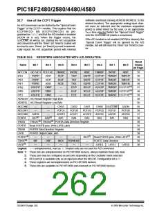
TABLE 20-2: REGISTERS ASSOCIATED WITH A/D OPERATION
Reset
Values
Name
Bit 7
Bit 6
Bit 5
Bit 4
Bit 3
Bit 2
Bit 1
Bit 0
on Page:
INTCON GIE/GIEH PEIE/GIEL TMR0IE
INT0IE
TXIP
TXIF
TXIE
EEIP
EEIF
EEIE
RBIE
SSPIP
SSPIF
SSPIE
BCLIP
BCLIF
BCLIE
TMR0IF
CCP1IP
CCP1IF
CCP1IE
HLVDIP
HLVDIF
HLVDIE
INT0IF
TMR2IP
TMR2IF
TMR2IE
TMR3IP ECCP1IP(5)
TMR3IF ECCP1IF(5)
TMR3IE ECCP1IE(5)
RBIF
55
58
58
58
57
58
58
56
56
56
56
57
58
58
58
58
58
58
58
58
IPR1
PIR1
PIE1
IPR2
PIR2
PIE2
PSPIP
PSPIF
ADIP
ADIF
ADIE
CMIP
CMIF
CMIE
RCIP
RCIF
RCIE
—
TMR1IP
TMR1IF
TMR1IE
PSPIE
OSCFIP
OSCFIF
OSCFIE
—
—
ADRESH A/D Result Register High Byte
ADRESL A/D Result Register Low Byte
ADCON0
ADCON1
ADCON2
PORTA
—
—
—
CHS3
VCFG1
ACQT2
RA5
CHS2
VCFG0
ACQT1
RA4
CHS1
PCFG3
ACQT0
RA3
CHS0 GO/DONE
ADON
PCFG0
ADCS0
RA0
—
PCFG2
ADCS2
RA2
PCFG1
ADCS1
RA1
ADFM
RA7(2)
—
RA6(2)
TRISA
TRISA7(2) TRISA6(2) PORTA Data Direction Register
PORTB Read PORTB pins, Write LATB Latch
TRISB
PORTB Data Direction Register
PORTB Output Data Latch
LATB
PORTE(4)
TRISE(4)
LATE(4)
—
IBF
—
—
OBF
—
—
IBOV
—
—
PSPMODE
—
RE3(3) Read PORTE pins, Write LATE(1)
—
—
PORTE Data Direction
LATE2 LATE1
LATE0
Legend: — = unimplemented, read as ‘0’. Shaded cells are not used for A/D conversion.
Note 1: These bits are unimplemented on PIC18F2X80 devices; always maintain these bits clear.
2: These pins may be configured as port pins depending on the Oscillator mode selected.
3: RE3 port bit is available only as an input pin when the MCLRE Configuration bit is ‘0’.
4: These registers are not implemented on PIC18F2X80 devices.
5: These bits are available on PIC18F4X80 and reserved on PIC18F2X80 devices.
DS39637D-page 262
© 2009 Microchip Technology Inc.

 MICROCHIP [ MICROCHIP ]