PIC18F2480/2580/4480/4580
changed, the comparator output level may not be valid
for the specified mode change delay shown in
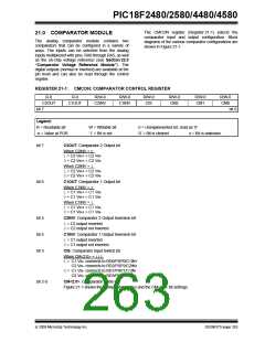
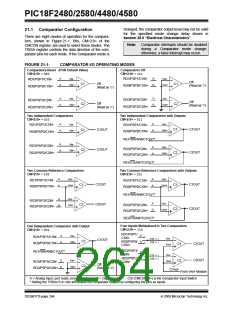
21.1 Comparator Configuration
There are eight modes of operation for the compara-
tors, shown in Figure 21-1. Bits, CM<2:0> of the
CMCON register, are used to select these modes. The
TRISA register controls the data direction of the com-
parator pins for each mode. If the Comparator mode is
Section 28.0 “Electrical Characteristics”.
Note: Comparator interrupts should be disabled
during
a
Comparator mode change;
otherwise, a false interrupt may occur.
FIGURE 21-1:
COMPARATOR I/O OPERATING MODES
Comparators Reset (POR Default Value)
Comparators Off
CM<2:0> = 000
CM<2:0> = 111
A
A
D
D
VIN-
RD1/PSP1/C1IN-
VIN-
RD1/PSP1/C1IN-
RD0/PSP0/C1IN+
Off
(Read as ‘
Off
C1
C2
C1
C2
VIN+
VIN+
RD0/PSP0/C1IN+
0
’)
(Read as ‘0’)
A
A
D
D
VIN-
VIN-
RD3/PSP3/C2IN-
RD2/PSP2/C2IN+
RD3/PSP3/C2IN-
RD2/PSP2/C2IN+
Off
(Read as ‘
Off
VIN+
VIN+
0’)
(Read as ‘0’)
Two Independent Comparators
Two Independent Comparators with Outputs
CM<2:0> = 010
CM<2:0> = 011
A
A
VIN-
A
A
VIN-
RD1/PSP1/C1IN-
RD0/PSP0/C1IN+
RD1/PSP1/C1IN-
RD0/PSP0/C1IN+
C1OUT
C2OUT
C1OUT
C2OUT
C1
C2
C1
C2
VIN+
VIN+
RE1/WR/AN6/C1OUT*
A
A
VIN-
RD3/PSP3/C2IN-
RD2/PSP2/C2IN+
A
VIN-
RD3/PSP3/C2IN-
VIN+
VIN+
A
RD2/PSP2/C2IN+
RE2/CS/AN7/C2OUT*
Two Common Reference Comparators
Two Common Reference Comparators with Outputs
CM<2:0> = 100
CM<2:0> = 101
A
A
A
A
VIN-
VIN-
RD1/PSP1/C1IN-
RD0/PSP0/C1IN+
RD1/PSP1/C1IN-
RD0/PSP0/C1IN+
C1OUT
C2OUT
C1OUT
C1
C2
C1
C2
VIN+
VIN+
RE1/WR/AN6/C1OUT*
A
D
VIN-
RD3/PSP3/C2IN-
RD2/PSP2/C2IN+
A
VIN-
RD3/PSP3/C2IN-
VIN+
C2OUT
VIN+
D
RD2/PSP2/C2IN+
RE2/CS/AN7/C2OUT*
Four Inputs Multiplexed to Two Comparators
One Independent Comparator with Output
CM<2:0> = 110
CM<2:0> = 001
RD1/PSP1/
A
A
A
VIN-
RD1/PSP1/C1IN-
RD0/PSP0/C1IN+
C1IN-
CIS = 0
CIS = 1
VIN-
C1OUT
C1
RD0/PSP0/
C1IN+
A
VIN+
C1OUT
C1
C2
VIN+
RD3/PSP3/
C2IN-
RD2/PSP2/
C2IN+
RE1/WR/AN6/C1OUT*
A
A
VIN-
CIS = 0
CIS = 1
C2OUT
D
VIN-
VIN+
RD3/PSP3/C2IN-
Off
(Read as ‘
C2
VIN+
D
RD2/PSP2/C2IN+
0’)
CVREF
From VREF Module
A = Analog Input, port reads zeros always
D = Digital Input
CIS (CMCON<3>) is the Comparator Input Switch
* Setting the TRISA<5:4> bits will disable the comparator outputs by configuring the pins as inputs.
DS39637D-page 264
© 2009 Microchip Technology Inc.

 MICROCHIP [ MICROCHIP ]