PIC18F2480/2580/4480/4580
20.2 Selecting and Configuring
Automatic Acquisition Time
20.3 Selecting the A/D Conversion
Clock
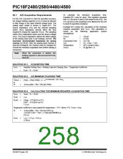
The ADCON2 register allows the user to select an
acquisition time that occurs each time the GO/DONE
bit is set.
The A/D conversion time per bit is defined as TAD. The
A/D conversion requires 11 TAD per 10-bit conversion.
The source of the A/D conversion clock is
software-selectable. There are seven possible options
for TAD:
When the GO/DONE bit is set, sampling is stopped and
a conversion begins. The user is responsible for ensur-
ing the required acquisition time has passed between
selecting the desired input channel and setting the
GO/DONE bit. This occurs when the ACQT<2:0> bits
(ADCON2<5:3>) remain in their Reset state (‘000’) and
is compatible with devices that do not offer
programmable acquisition times.
• 2 TOSC
• 4 TOSC
• 8 TOSC
• 16 TOSC
• 32 TOSC
• 64 TOSC
If desired, the ACQT bits can be set to select a
programmable acquisition time for the A/D module.
When the GO/DONE bit is set, the A/D module
continues to sample the input for the selected acquisition
time, then automatically begins a conversion. Since the
acquisition time is programmed, there may be no need
to wait for an acquisition time between selecting a
channel and setting the GO/DONE bit.
• Internal RC Oscillator
For correct A/D conversions, the A/D conversion clock
(TAD) must be as short as possible, but greater than the
minimum TAD (approximately 2 μs, see parameter 130
for more information).
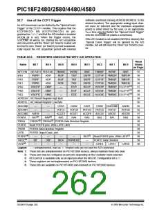
Table 20-1 shows the resultant TAD times derived from
the device operating frequencies and the A/D clock
source selected.
In either case, when the conversion is completed, the
GO/DONE bit is cleared, the ADIF flag is set and the
A/D begins sampling the currently selected channel
again. If an acquisition time is programmed, there is
nothing to indicate if the acquisition time has ended or
if the conversion has begun.
TABLE 20-1: TAD vs. DEVICE OPERATING FREQUENCIES
AD Clock Source (TAD)
Maximum Device Frequency
Operation
ADCS2:ADCS0
PIC18F2X80/4X80
PIC18LF2X80/4X80(4)
2 TOSC
4 TOSC
8 TOSC
16 TOSC
32 TOSC
64 TOSC
RC(3)
000
100
001
101
010
110
x11
2.86 MHz
5.71 MHz
11.43 MHz
22.86 MHz
40.0 MHz
40.0 MHz
1.00 MHz(1)
1.43 kHz
2.86 MHz
5.72 MHz
11.43 MHz
22.86 MHz
22.86 MHz
1.00 MHz(2)
Note 1: The RC source has a typical TAD time of 1.2 ms.
2: The RC source has a typical TAD time of 2.5 ms.
3: For device frequencies above 1 MHz, the device must be in Sleep for the entire conversion or the A/D
accuracy may be out of specification.
4: Low-power (PIC18LFXXXX) devices only.
© 2009 Microchip Technology Inc.
DS39637D-page 259

 MICROCHIP [ MICROCHIP ]