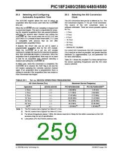
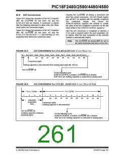
PIC18F2480/2580/4480/4580
To calculate the minimum acquisition time,
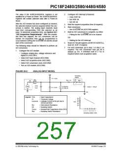
20.1 A/D Acquisition Requirements
Equation 20-1 may be used. This equation assumes
that 1/2 LSb error is used (1024 steps for the A/D). The
1/2 LSb error is the maximum error allowed for the A/D
to meet its specified resolution.
For the A/D Converter to meet its specified accuracy,
the charge holding capacitor (CHOLD) must be allowed
to fully charge to the input channel voltage level. The
analog input model is shown in Figure 20-2. The
source impedance (RS) and the internal sampling
switch (RSS) impedance directly affect the time
required to charge the capacitor CHOLD. The sampling
switch (RSS) impedance varies over the device voltage
(VDD). The source impedance affects the offset voltage
at the analog input (due to pin leakage current). The
maximum recommended impedance for analog
sources is 2.5 kΩ. After the analog input channel is
selected (changed), the channel must be sampled for
at least the minimum acquisition time before starting a
conversion.
Example 20-3 shows the calculation of the minimum
required acquisition time TACQ. This calculation is
based on the following application system
assumptions:
CHOLD
Rs
Conversion Error
VDD
Temperature
VHOLD
=
=
≤
=
=
=
120 pF
2.5 kΩ
1/2 LSb
5V → Rss = 7 kΩ
50°C (system max.)
0V @ time = 0
Note:
When the conversion is started, the
holding capacitor is disconnected from the
input pin.
EQUATION 20-1: ACQUISITION TIME
TACQ
=
=
Amplifier Settling Time + Holding Capacitor Charging Time + Temperature Coefficient
TAMP + TC + TCOFF
EQUATION 20-2: A/D MINIMUM CHARGING TIME
VHOLD =
or
(VREF – (VREF/2048)) • (1 – e(-Tc/CHOLD(RIC + RSS + RS))
)
TC
=
-(CHOLD)(RIC + RSS + RS) ln(1/2048)
EQUATION 20-3: CALCULATING THE MINIMUM REQUIRED ACQUISITION TIME
TACQ
TAMP
TCOFF
=
=
=
TAMP + TC + TCOFF
5 μs
(Temp – 25°C)(0.05 μs/°C)
(50°C – 25°C)(0.05 μs/°C)
1.25 μs
Temperature coefficient is only required for temperatures > 25°C. Below 25°C, TCOFF = 0 ms.
TC
=
-(CHOLD)(RIC + RSS + RS) ln(1/2047) μs
-(120 pF) (1 kΩ + 7 kΩ + 2.5 kΩ) ln(0.0004883) μs
9.61 μs
TACQ
=
5 μs + 1.25 μs + 9.61 μs
12.86 μs
DS39637D-page 258
© 2009 Microchip Technology Inc.

 MICROCHIP [ MICROCHIP ]