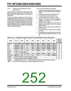
PIC18F2480/2580/4480/4580
Once the TXREG register transfers the data to the TSR
19.3 EUSART Synchronous
Master Mode
register (occurs in one TCYCLE), the TXREG is empty
and the TXIF flag bit (PIR1<4>) is set. The interrupt can
be enabled or disabled by setting or clearing the inter-
rupt enable bit, TXIE (PIE1<4>). TXIF is set regardless
of the state of enable bit TXIE; it cannot be cleared in
software. It will reset only when new data is loaded into
the TXREG register.
The Master mode indicates that the processor trans-
mits the master clock on the CK line. The Synchronous
Master mode is entered by setting the CSRC bit
(TXSTA<7>). In this mode, the data is transmitted in a
half-duplex manner (i.e., transmission and reception do
not occur at the same time). When transmitting data,
the reception is inhibited and vice versa. Synchronous
mode is entered by setting bit, SYNC (TXSTA<4>). In
addition, enable bit, SPEN (RCSTA<7>), is set in order
to configure the TX and RX pins to CK (clock) and DT
(data) lines, respectively.
While flag bit, TXIF, indicates the status of the TXREG
register, another bit, TRMT (TXSTA<1>), shows the
status of the TSR register. TRMT is a read-only bit which
is set when the TSR is empty. No interrupt logic is tied to
this bit so the user has to poll this bit in order to
determine if the TSR register is empty. The TSR is not
mapped in data memory so it is not available to the user.
The Master mode indicates that the processor trans-
mits the master clock on the CK line. Clock polarity is
selected with the SCKP bit (BAUDCON<4>). Setting
SCKP sets the Idle state on CK as high, while clearing
the bit sets the Idle state as low. This option is provided
to support Microwire devices with this module.
To set up a Synchronous Master Transmission:
1. Initialize the SPBRGH:SPBRG registers for the
appropriate baud rate. Set or clear the BRG16
bit, as required, to achieve the desired baud
rate.
19.3.1
EUSART SYNCHRONOUS MASTER
TRANSMISSION
2. Enable the synchronous master serial port by
setting bits, SYNC, SPEN and CSRC.
3. If interrupts are desired, set enable bit, TXIE.
4. If 9-bit transmission is desired, set bit, TX9.
5. Enable the transmission by setting bit, TXEN.
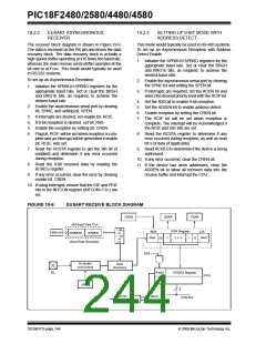
The EUSART transmitter block diagram is shown in
Figure 19-3. The heart of the transmitter is the Transmit
(Serial) Shift Register (TSR). The Shift register obtains
its data from the Read/Write Transmit Buffer register,
TXREG. The TXREG register is loaded with data in
software. The TSR register is not loaded until the last
bit has been transmitted from the previous load. As
soon as the last bit is transmitted, the TSR is loaded
with new data from the TXREG (if available).
6. If 9-bit transmission is selected, the ninth bit
should be loaded in bit, TX9D.
7. Start transmission by loading data to the TXREG
register.
8. If using interrupts, ensure that the GIE and PEIE
bits in the INTCON register (INTCON<7:6>) are
set.
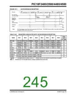
FIGURE 19-11:
SYNCHRONOUS TRANSMISSION
Q1 Q2 Q3Q4 Q1 Q2 Q3 Q4 Q1Q2 Q3 Q4 Q1Q2 Q3 Q4Q1 Q2 Q3 Q4
Q3 Q4 Q1 Q2 Q3Q4 Q1Q2 Q3Q4 Q1 Q2Q3Q4 Q1 Q2Q3 Q4Q1 Q2 Q3 Q4 Q1 Q2 Q3 Q4
RC7/RX/DT
pin
bit 0
bit 1
bit 2
bit 7
bit 0
bit 1
bit 7
Word 2
Word 1
RC6/TX/CK pin
(SCKP = 0)
RC6/TX/CK pin
(SCKP = 1)
Write to
TXREG Reg
Write Word 1
Write Word 2
TXIF bit
(Interrupt Flag)
TRMT bit
‘1’
‘1’
TXEN bit
Note: Sync Master mode, SPBRG = 0, continuous transmission of two 8-bit words.
DS39637D-page 248
© 2009 Microchip Technology Inc.

 MICROCHIP [ MICROCHIP ]