PIC18F2480/2580/4480/4580
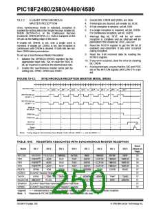
3. Ensure bits, CREN and SREN, are clear.
4. If interrupts are desired, set enable bit, RCIE.
5. If 9-bit reception is desired, set bit, RX9.
19.3.2
EUSART SYNCHRONOUS
MASTER RECEPTION
Once Synchronous mode is selected, reception is
enabled by setting either the Single Receive Enable bit,
SREN (RCSTA<5>), or the Continuous Receive
Enable bit, CREN (RCSTA<4>). Data is sampled on the
RX pin on the falling edge of the clock.
6. If a single reception is required, set bit, SREN.
For continuous reception, set bit, CREN.
7. Interrupt flag bit, RCIF, will be set when
reception is complete and an interrupt will be
generated if the enable bit, RCIE, was set.
If enable bit, SREN, is set, only a single word is
received. If enable bit, CREN, is set, the reception is
continuous until CREN is cleared. If both bits are set,
then CREN takes precedence.
8. Read the RCSTA register to get the 9th bit (if
enabled) and determine if any error occurred
during reception.
9. Read the 8-bit received data by reading the
RCREG register.
To set up a Synchronous Master Reception:
1. Initialize the SPBRGH:SPBRG registers for the
appropriate baud rate. Set or clear the BRG16
bit, as required, to achieve the desired baud rate.
10. If any error occurred, clear the error by clearing
bit, CREN.
11. If using interrupts, ensure that the GIE and PEIE
bits in the INTCON register (INTCON<7:6>) are
set.
2. Enable the synchronous master serial port by
setting bits, SYNC, SPEN and CSRC.
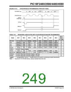
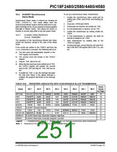
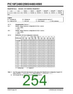
FIGURE 19-13:
SYNCHRONOUS RECEPTION (MASTER MODE, SREN)
Q2 Q3 Q4 Q1 Q2 Q3 Q4 Q1 Q2 Q3 Q4 Q1 Q2 Q3 Q4 Q1 Q2 Q3 Q4 Q1 Q2 Q3 Q4Q1 Q2 Q3 Q4 Q1Q2 Q3 Q4 Q1 Q2 Q3 Q4 Q1 Q2 Q3 Q4 Q1 Q2 Q3 Q4
RC7/RX1/DT1
pin
bit 0
bit 1
bit 2
bit 3
bit 4
bit 5
bit 6
bit 7
RC7/TX/CK pin
(SCKP = 0)
RC7/TX/CK pin
(SCKP = 1)
Write to
bit SREN
SREN bit
CREN bit
‘0’
‘0’
RCIF bit
(Interrupt)
Read
RXREG
Note: Timing diagram demonstrates Sync Master mode with bit, SREN = 1, and bit, BRGH = 0.
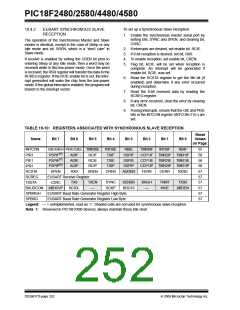
TABLE 19-8: REGISTERS ASSOCIATED WITH SYNCHRONOUS MASTER RECEPTION
Reset
Values on
Page:
Name
Bit 7
Bit 6
Bit 5
Bit 4
Bit 3
Bit 2
Bit 1
Bit 0
INTCON
PIR1
GIE/GIEH PEIE/GIEL
TMR0IE
RCIF
INT0IE
TXIF
RBIE
SSPIF
SSPIE
SSPIP
ADDEN
TMR0IF
CCP1IF
CCP1IE
CCP1IP
FERR
INT0IF
TMR2IF
TMR2IE
TMR2IP
OERR
RBIF
55
58
58
58
57
57
57
57
57
57
(1)
PSPIF
PSPIE
PSPIP
ADIF
ADIE
ADIP
RX9
TMR1IF
TMR1IE
TMR1IP
RX9D
(1)
(1)
PIE1
RCIE
TXIE
IPR1
RCIP
TXIP
RCSTA
RCREG
TXSTA
BAUDCON
SPBRGH
SPBRG
Legend:
SPEN
SREN
CREN
EUSART Receive Register
CSRC
TX9
TXEN
—
SYNC
SCKP
SENDB
BRG16
BRGH
—
TRMT
WUE
TX9D
ABDOVF
RCIDL
ABDEN
EUSART Baud Rate Generator Register High Byte
EUSART Baud Rate Generator Register Low Byte
— = unimplemented, read as ‘0’. Shaded cells are not used for synchronous master reception.
Note 1: Reserved in PIC18F2X80 devices; always maintain these bits clear.
DS39637D-page 250
© 2009 Microchip Technology Inc.

 MICROCHIP [ MICROCHIP ]