PIC18F2450/4450
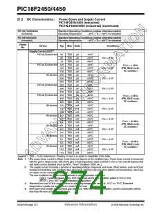
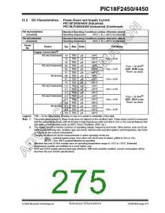
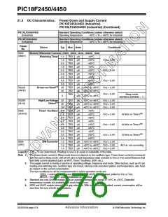
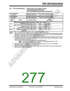
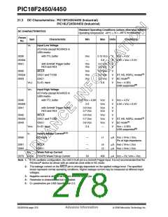
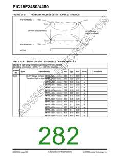
21.3 DC Characteristics: PIC18F2450/4450 (Industrial)
PIC18LF2450/4450 (Industrial)
Standard Operating Conditions (unless otherwise stated)
Operating temperature -40°C ≤ TA ≤ +85°C for industrial
DC CHARACTERISTICS
Param
Sym
No.
Characteristic
Min
Max
Units
Conditions
VIL
Input Low Voltage
I/O Ports (except RC4/RC5 in
USB mode):
D030
D030A
D031
with TTL buffer
VSS
—
0.15 VDD
0.8
V
V
VDD < 4.5V
4.5V ≤ VDD ≤ 5.5V
with Schmitt Trigger buffer
RC3 and RC4
VSS
VSS
0.2 VDD
0.3 VDD
V
V
D032
D032A
D033
MCLR
VSS
VSS
VSS
—
0.2 VDD
0.3 VDD
0.2 VDD
0.8
V
V
V
V
OSC1 and T1OSI
OSC1
XT, HS, HSPLL modes(1)
EC mode(1)
VILU
VIH
D+/D- Input
VDD = 4.35V,
USB suspended(5)
Input High Voltage
I/O Ports (except RC4/RC5 in
USB mode):
D040
D040A
D041
with TTL buffer
0.25 VDD + 0.8V
2.0
VDD
VDD
V
V
VDD < 4.5V
4.5V ≤ VDD ≤ 5.5V
with Schmitt Trigger buffer
RC3 and RC4
0.8 VDD
0.7 VDD
VDD
VDD
V
V
D042
D042A
D043
MCLR
0.8 VDD
0.7 VDD
0.8 VDD
2.4
VDD
VDD
VDD
—
V
V
V
V
OSC1 and T1OSI
OSC1
XT, HS, HSPLL modes(1)
EC mode(1)
VIHU
IIL
D+/D- Input
VDD = 4.35V,
USB suspended(5)
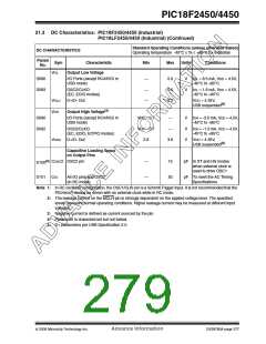
Input Leakage Current(2,3)
D060
I/O Ports
—
1
μA VSS ≤ VPIN ≤ VDD,
Pin at high-impedance
D061
D063
MCLR
—
—
5
5
μA Vss ≤ VPIN ≤ VDD
μA Vss ≤ VPIN ≤ VDD
OSC1
IPU
Weak Pull-up Current
PORTB Weak Pull-up Current
D070
IPURB
50
400
μA VDD = 5V, VPIN = VSS
Note 1: In RC oscillator configuration, the OSC1/CLKI pin is a Schmitt Trigger input. It is not recommended that the
PICmicro® device be driven with an external clock while in RC mode.
2: The leakage current on the MCLR pin is strongly dependent on the applied voltage level. The specified
levels represent normal operating conditions. Higher leakage current may be measured at different input
voltages.
3: Negative current is defined as current sourced by the pin.
4: Parameter is characterized but not tested.
5: D+ parameters per USB Specification 2.0.
DS39760A-page 276
Advance Information
© 2006 Microchip Technology Inc.

 MICROCHIP [ MICROCHIP ]