PIC18F2450/4450
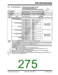
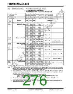
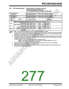
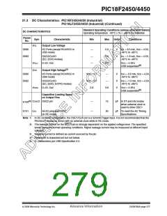
21.3 DC Characteristics: PIC18F2450/4450 (Industrial)
PIC18LF2450/4450 (Industrial) (Continued)
Standard Operating Conditions (unless otherwise stated)
Operating temperature -40°C ≤ TA ≤ +85°C for industrial
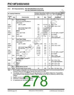
DC CHARACTERISTICS
Param
Sym
No.
Characteristic
Min
Max
Units
Conditions
VOL
Output Low Voltage
D080
D083
I/O Ports (except RC4/RC5 in
USB mode)
—
—
—
0.6
0.6
0.3
V
V
IOL = 8.5 mA, VDD = 4.5V,
-40°C to +85°C
OSC2/CLKO
(EC, ECIO modes)
IOL = 1.6 mA, VDD = 4.5V,
-40°C to +85°C
VOLU
VOH
D+/D- Out
VDD = 4.35V,
USB suspended(5)
Output High Voltage(3)
D090
D092
I/O Ports (except RC4/RC5 in
USB mode)
VDD – 0.7
VDD – 0.7
2.8
—
—
V
V
V
IOH = -3.0 mA, VDD = 4.5V,
-40°C to +85°C
OSC2/CLKO
(EC, ECIO, ECPIO modes)
IOH = -1.3 mA, VDD = 4.5V,
-40°C to +85°C
VOHU
D+/D- Out
3.6
VDD = 4.35V,
USB suspended(5)
Capacitive Loading Specs
on Output Pins
D100(4)
D101
COSC2 OSC2 pin
—
—
15
50
pF In XT and HS modes
when external clock is
used to drive OSC1
CIO
All I/O pins and OSC2
(in RC mode)
pF To meet the AC Timing
Specifications
Note 1: In RC oscillator configuration, the OSC1/CLKI pin is a Schmitt Trigger input. It is not recommended that the
PICmicro® device be driven with an external clock while in RC mode.
2: The leakage current on the MCLR pin is strongly dependent on the applied voltage level. The specified
levels represent normal operating conditions. Higher leakage current may be measured at different input
voltages.
3: Negative current is defined as current sourced by the pin.
4: Parameter is characterized but not tested.
5: D+ parameters per USB Specification 2.0.
© 2006 Microchip Technology Inc.
Advance Information
DS39760A-page 277

 MICROCHIP [ MICROCHIP ]