PIC18F2450/4450
(moving ADRESH:ADRESL to the desired location).
The appropriate analog input channel must be selected
and the minimum acquisition period is either timed by
the user, or an appropriate TACQ time selected before
the Special Event Trigger sets the GO/DONE bit (starts
a conversion).
16.8 Use of the CCP1 Trigger
An A/D conversion can be started by the Special Event
Trigger of the CCP1 module. This requires that the
CCP1M3:CCP1M0
bits
(CCP1CON<3:0>)
be
programmed as ‘1011’ and that the A/D module is
enabled (ADON bit is set). When the trigger occurs, the
GO/DONE bit will be set, starting the A/D acquisition
and conversion and the Timer1 counter will be reset to
zero. Timer1 is reset to automatically repeat the A/D
acquisition period with minimal software overhead
If the A/D module is not enabled (ADON is cleared), the
Special Event Trigger will be ignored by the A/D
module but will still reset the Timer1 counter.
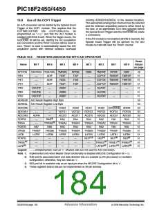
TABLE 16-2: REGISTERS ASSOCIATED WITH A/D OPERATION
Reset
Values
on page
Name
Bit 7
Bit 6
Bit 5
Bit 4
Bit 3
Bit 2
Bit 1
Bit 0
INTCON
PIR1
PIE1
GIE/GIEH PEIE/GIEL TMR0IE
INT0IE
TXIF
RBIE
—
TMR0IF
CCP1IF
CCP1IE
CCP1IP
HLVDIF
HLVDIE
HLVDIP
INT0IF
TMR2IF
TMR2IE
TMR2IP
RBIF
49
51
51
51
51
51
51
50
50
50
50
50
51
51
51
51
51
51
51
51
ADIF
ADIE
ADIP
—
RCIF
RCIE
TMR1IF
TMR1IE
TMR1IP
—
—
TXIE
TXIP
—
IPR1
PIR2
PIE2
RCIP
—
—
OSCFIF
OSCFIE
OSCFIP
USBIF
USBIE
USBIP
—
—
—
—
—
—
—
—
—
—
—
—
IPR2
—
—
ADRESH A/D Result Register High Byte
ADRESL A/D Result Register Low Byte
ADCON0
ADCON1
ADCON2
PORTA
TRISA
—
—
—
—
CHS3
VCFG1
ACQT2
RA5
CHS2
VCFG0
ACQT1
RA4
CHS1
PCFG3
ACQT0
RA3
CHS0 GO/DONE ADON
PCFG2
ADCS2
RA2
PCFG1
ADCS1
RA1
PCFG0
ADCS0
RA0
ADFM
—
—
RA6(2)
—
TRISA6(2) TRISA5
TRISA4
RB4
TRISA3
RB3
TRISA2
RB2
TRISA1
RB1
TRISA0
RB0
PORTB
TRISB
RB7
TRISB7
LATB7
—
RB6
TRISB6
LATB6
—
RB5
TRISB5
LATB5
—
TRISB4
LATB4
—
TRISB3
LATB3
RE3(1,3)
—
TRISB2
LATB2
RE2(4)
TRISB1
LATB1
RE1(4)
TRISB0
LATB0
RE0(4)
LATB
PORTE
TRISE(4)
LATE(4)
—
—
—
—
TRISE2(4) TRISE1(4) TRISE0(4)
LATE2(4) LATE1(4) LATE0(4)
—
—
—
—
—
Legend: — = unimplemented, read as ‘0’. Shaded cells are not used for A/D conversion.
Note 1: Implemented only when Master Clear functionality is disabled (MCLRE Configuration bit = 0).
2: RA6 and its associated latch and data direction bits are enabled as I/O pins based on oscillator
configuration; otherwise, they are read as ‘0’.
3: RE3 port bit is available only as an input pin when the MCLRE Configuration bit is ‘0’.
4: These registers and/or bits are not implemented on 28-pin devices.
DS39760A-page 182
Advance Information
© 2006 Microchip Technology Inc.

 MICROCHIP [ MICROCHIP ]