PIC18F2450/4450
After the A/D conversion is completed or aborted, a
2 TAD wait is required before the next acquisition can be
started. After this wait, acquisition on the selected
channel is automatically started.
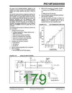
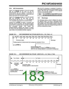
16.6 A/D Conversions
Figure 16-4 shows the operation of the A/D converter
after the GO/DONE bit has been set and the
ACQT2:ACQT0 bits are cleared. A conversion is
started after the following instruction to allow entry into
Sleep mode before the conversion begins.
Note:
The GO/DONE bit should NOT be set in
the same instruction that turns on the A/D.
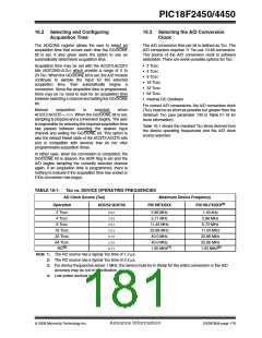
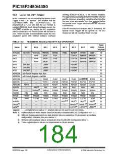
Figure 16-5 shows the operation of the A/D converter
after the GO/DONE bit has been set, the
ACQT2:ACQT0 bits are set to ‘010’ and selecting a
4 TAD acquisition time before the conversion starts.
16.7 Discharge
The discharge phase is used to initialize the value of
the capacitor array. The array is discharged before
every sample. This feature helps to optimize the unity-
gain amplifier as the circuit always needs to charge the
capacitor array, rather than charge/discharge based on
previous measurement values.
Clearing the GO/DONE bit during a conversion will
abort the current conversion. The A/D Result register
pair will NOT be updated with the partially completed
A/D
conversion
sample.
This
means
the
ADRESH:ADRESL registers will continue to contain
the value of the last completed conversion (or the last
value written to the ADRESH:ADRESL registers).
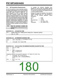
FIGURE 16-4:
A/D CONVERSION TAD CYCLES (ACQT<2:0> = 000, TACQ = 0)
TCY - TAD
TAD6 TAD7 TAD8 TAD9 TAD10 TAD11 TAD1
TAD1 TAD2 TAD3 TAD4 TAD5
b7
b6
b4
b1
b0
b9
b8
b5
b3
b2
Conversion starts
Discharge
Holding capacitor is disconnected from analog input (typically 100 ns)
Set GO/DONE bit
On the following cycle:
ADRESH:ADRESL is loaded, GO/DONE bit is cleared,
ADIF bit is set, holding capacitor is connected to analog input.
FIGURE 16-5:
A/D CONVERSION TAD CYCLES (ACQT<2:0> = 010, TACQ = 4 TAD)
TACQ Cycles
TAD Cycles
7
8
9
10
b1
11 TAD1
b0
1
2
3
4
1
2
3
4
5
6
b7
b6
b3
b2
b8
b5
b4
b9
Automatic
Acquisition
Time
Discharge
Conversion starts
(Holding capacitor is disconnected)
Set GO/DONE bit
(Holding capacitor continues
acquiring input)
On the following cycle:
ADRESH:ADRESL is loaded, GO/DONE bit is cleared,
ADIF bit is set, holding capacitor is connected to analog input.
© 2006 Microchip Technology Inc.
Advance Information
DS39760A-page 181

 MICROCHIP [ MICROCHIP ]