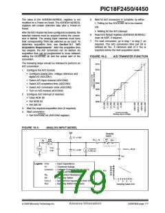
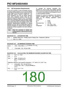
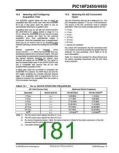
PIC18F2450/4450
16.4 Operation in Power-Managed
Modes
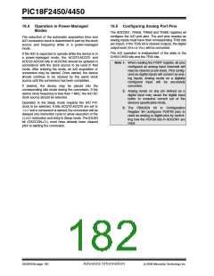
16.5 Configuring Analog Port Pins
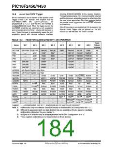
The ADCON1, TRISA, TRISB and TRISE registers all
configure the A/D port pins. The port pins needed as
analog inputs must have their corresponding TRIS bits
set (input). If the TRIS bit is cleared (output), the digital
output level (VOH or VOL) will be converted.
The selection of the automatic acquisition time and
A/D conversion clock is determined in part by the clock
source and frequency while in a power-managed
mode.
The A/D operation is independent of the state of the
CHS3:CHS0 bits and the TRIS bits.
If the A/D is expected to operate while the device is in
a power-managed mode, the ACQT2:ACQT0 and
ADCS2:ADCS0 bits in ADCON2 should be updated in
accordance with the clock source to be used in that
mode. After entering the mode, an A/D acquisition or
conversion may be started. Once started, the device
should continue to be clocked by the same clock
source until the conversion has been completed.
Note 1: When reading the PORT register, all pins
configured as analog input channels will
read as cleared (a low level). Pins config-
ured as digital inputs will convert as ana-
log inputs. Analog levels on a digitally
configured input will be accurately
converted.
If desired, the device may be placed into the
corresponding Idle mode during the conversion. If the
device clock frequency is less than 1 MHz, the A/D RC
clock source should be selected.
2: Analog levels on any pin defined as a
digital input may cause the digital input
buffer to consume current out of the
device’s specification limits.
Operation in the Sleep mode requires the A/D FRC
clock to be selected. If bits ACQT2:ACQT0 are set to
‘000’ and a conversion is started, the conversion will be
delayed one instruction cycle to allow execution of the
SLEEPinstruction and entry to Sleep mode. The IDLEN
bit (OSCCON<7>) must have already been cleared
prior to starting the conversion.
3: The PBADEN bit in Configuration
Register 3H configures PORTB pins to
reset as analog or digital pins by control-
ling how the PCFG0 bits in ADCON1 are
reset.
DS39760A-page 180
Advance Information
© 2006 Microchip Technology Inc.

 MICROCHIP [ MICROCHIP ]