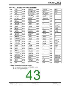
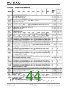
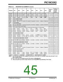
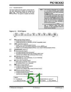
PIC18CXX2
If the currently selected bank is not implemented, any
read will return all '0's and all writes are ignored. The
STATUS register bits will be set/cleared as appropriate
for the instruction performed.
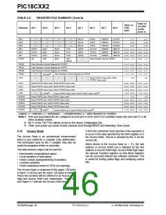
4.11
Bank Select Register (BSR)
The need for a large general purpose memory space
dictates a RAM banking scheme. The data memory is
partitioned into sixteen banks. When using direct
addressing, the BSR should be configured for the
desired bank.
Each Bank extends up to FFh (256 bytes). All data
memory is implemented as static RAM.
A MOVFF instruction ignores the BSR, since the 12-bit
addresses are embedded into the instruction word.
BSR<3:0> holds the upper 4 bits of the 12-bit RAM
address. The BSR<7:4> bits will always read ’0’s, and
writes will have no effect.
Section 4.12 provides a description of indirect address-
ing, which allows linear addressing of the entire RAM
space.
A MOVLB instruction has been provided in the instruc-
tion set to assist in selecting banks.
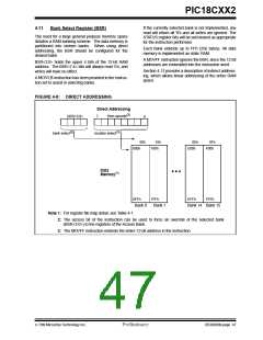
FIGURE 4-8: DIRECT ADDRESSING
Direct Addressing
(3)
from opcode
BSR<3:0>
7
0
(2)
(3)
bank select
location select
00h
000h
01h
100h
0Eh
E00h
0Fh
F00h
Data
Memory(1)
0FFh
1FFh
EFFh
FFFh
Bank 0
Bank 1
Bank 14 Bank 15
Note 1: For register file map detail, see Table 4-1.
2: The access bit of the instruction can be used to force an override of the selected bank
(BSR<3:0>) to the registers of the Access Bank.
3: The MOVFF instruction embeds the entire 12-bit address in the instruction.
7/99 Microchip Technology Inc.
Preliminary
DS39026B-page 47

 MICROCHIP [ MICROCHIP ]