PIC18CXX2
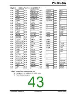
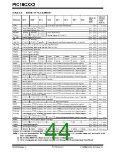
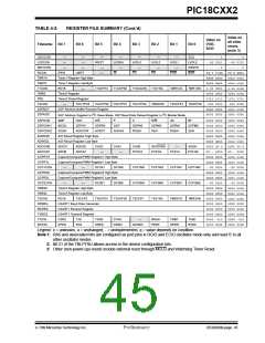
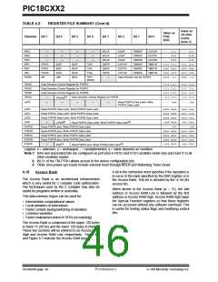
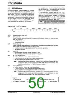
TABLE 4-2:
REGISTER FILE SUMMARY (Cont.’d)
Value on
all other
resets
Value on
POR,
BOR
Filename
Bit 7
Bit 6
Bit 5
Bit 4
Bit 3
Bit 2
Bit 1
Bit 0
(note 3)
IPR2
PIR2
PIE2
IPR1
PIR1
PIE1
TRISE
—
—
—
—
BCLIP
BCLIF
BCLIE
SSPIP
SSPIF
SSPIE
—
LVDIP
TMR3IP
TMR3IF
TMR3IE
TMR2IP
TMR2IF
TMR2IE
CCP2IP
CCP2IF
CCP2IE
TMR1IP
TMR1IF
TMR1IE
---- 1111
---- 0000
---- 0000
1111 1111
0000 0000
0000 0000
0000 -111
---- 1111
---- 0000
---- 0000
1111 1111
0000 0000
0000 0000
0000 -111
—
—
—
—
—
—
—
—
LVDIF
LVDIE
PSPIP
PSPIF
PSPIE
IBF
ADIP
RCIP
TXIP
CCP1IP
CCP1IF
CCP1IE
ADIF
ADIE
OBF
RCIF
RCIE
IBOV
TXIF
TXIE
PSP-
Data Direction bits for PORTE
MODE
TRISD
TRISC
TRISB
TRISA
Data Direction Control Register for PORTD
Data Direction Control Register for PORTC
Data Direction Control Register for PORTB
1111 1111
1111 1111
1111 1111
-111 1111
1111 1111
1111 1111
1111 1111
-111 1111
TRISA6(1)
—
—
—
Data Direction Control Register for PORTA
LATE
—
—
—
Read PORTE Data Latch, Write
PORTE Data Latch
---- -xxx
---- -uuu
LATD
LATC
LATB
LATA
Read PORTD Data Latch, Write PORTD Data Latch
Read PORTC Data Latch, Write PORTC Data Latch
Read PORTB Data Latch, Write PORTB Data Latch
—
xxxx xxxx
xxxx xxxx
xxxx xxxx
-xxx xxxx
uuuu uuuu
uuuu uuuu
uuuu uuuu
-uuu uuuu
LATA6(1)
Read PORTA Data Latch, Write PORTA Data Latch(1)
PORTE
PORTD
PORTC
PORTB
PORTA
Read PORTE pins, Write PORTE Data Latch
Read PORTD pins, Write PORTD Data Latch
Read PORTC pins, Write PORTC Data Latch
Read PORTB pins, Write PORTB Data Latch
—
---- -000
xxxx xxxx
xxxx xxxx
xxxx xxxx
-x0x 0000
---- -000
uuuu uuuu
uuuu uuuu
uuuu uuuu
-u0u 0000
RA6(1)
Read PORTA pins, Write PORTA Data Latch(1)
Legend: x = unknown, u = unchanged, - = unimplemented, q = value depends on condition
Note 1: RA6 and associated bits are configured as port pins in RCIO and ECIO oscillator mode only and read ’0’ in all
other oscillator modes.
2: Bit 21 of the TBLPTRU allows access to the device configuration bits.
3: Other (non-power-up) resets include external reset through MCLR and Watchdog Timer Reset.
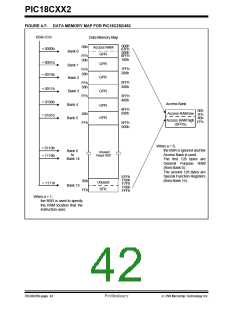
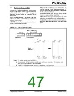
A bit in the instruction word specifies if the operation is
to occur in the bank specified by the BSR register or in
the Access Bank. This bit is denoted by the ’a’ bit (for
access bit).
4.10
Access Bank
The Access Bank is an architectural enhancement
which is very useful for C compiler code optimization.
The techniques used by the C compiler may also be
useful for programs written in assembly.
When forced in the Access Bank (a = ’0’), the last
address in Access RAM Low is followed by the first
address in Access RAM High. Access RAM High maps
the Special Function registers so that these registers
can be accessed without any software overhead. This
is useful for testing status flags and modifying control
bits.
This data memory region can be used for:
• Intermediate computational values
• Local variables of subroutines
• Faster context saving/switching of variables
• Common variables
• Faster evaluation/control of SFRs (no banking)
The Access Bank is comprised of the upper 128 bytes
in Bank 15 (SFRs) and the lower 128 bytes in Bank 0.
These two sections will be referred to as Access RAM
High and Access RAM Low, respectively. Figure 4-6
and Figure 4-7 indicate the Access RAM areas.
DS39026B-page 46
Preliminary
7/99 Microchip Technology Inc.

 MICROCHIP [ MICROCHIP ]