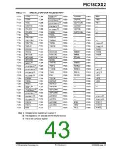
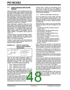
PIC18CXX2
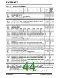
TABLE 4-2:
REGISTER FILE SUMMARY
Value on
all other
resets
Value on
POR,
BOR
Filename
Bit 7
Bit 6
Bit 5
Bit 4
Bit 3
Bit 2
Bit 1
Bit 0
(note 3)
TOSU
—
—
—
Top-of-Stack upper Byte (TOS<20:16>)
---0 0000
0000 0000
0000 0000
00-0 0000
---0 0000
0000 0000
0000 0000
---0 0000
---0 0000
0000 0000
0000 0000
00-0 0000
---0 0000
0000 0000
0000 0000
---0 0000
TOSH
Top-of-Stack High Byte (TOS<15:8>)
Top-of-Stack Low Byte (TOS<7:0>)
TOSL
STKPTR
PCLATU
PCLATH
PCL
STKFUL
—
STKUNF
—
—
—
Return Stack Pointer
Holding Register for PC<20:16>
Holding Register for PC<15:8>
PC Low Byte (PC<7:0>)
bit21(2)
TBLPTRU
—
—
Program Memory Table Pointer Upper Byte (TBLPTR<20:16>)
TBLPTRH
TBLPTRL
TABLAT
Program Memory Table Pointer High Byte (TBLPTR<15:8>)
Program Memory Table Pointer Low Byte (TBLPTR<7:0>)
Program Memory Table Latch
0000 0000
0000 0000
0000 0000
xxxx xxxx
xxxx xxxx
0000 000x
1111 -1-1
11-0 0-00
n/a
0000 0000
0000 0000
0000 0000
uuuu uuuu
uuuu uuuu
0000 000u
1111 -1-1
11-0 0-00
n/a
PRODH
Product Register High Byte
PRODL
Product Register Low Byte
INTCON
INTCON2
INTCON3
INDF0
GIE/GIEH PEIE/GIEL TMR0IE
INT0IE
RBIE
TMR0IF
TMR0IP
—
INT0IF
—
RBIF
RBPU
INTEDG0
INT1IP
INTEDG1
—
INTEDG2
INT2IE
—
RBIP
INT1IF
INT2IP
INT1IE
INT2IF
Uses contents of FSR0 to address data memory - value of FSR0 not changed (not a physical register)
Uses contents of FSR0 to address data memory - value of FSR0 post-incremented (not a physical register)
POSTINC0
n/a
n/a
POSTDEC0 Uses contents of FSR0 to address data memory - value of FSR0 post-decremented (not a physical register) n/a
n/a
PREINC0
PLUSW0
Uses contents of FSR0 to address data memory - value of FSR0 pre-incremented (not a physical register)
n/a
n/a
n/a
Uses contents of FSR0 to address data memory - value of FSR0 pre-incremented (not a physical register) -
value of FSR0 offset by value in WREG
n/a
FSR0H
FSR0L
—
—
—
—
Indirect Data Memory Address Pointer 0 High Byte
---- 0000
xxxx xxxx
xxxx xxxx
n/a
---- 0000
Indirect Data Memory Address Pointer 0 Low Byte
Working Register
uuuu uuuu
WREG
uuuu uuuu
INDF1
Uses contents of FSR1 to address data memory - value of FSR1 not changed (not a physical register)
Uses contents of FSR1 to address data memory - value of FSR1 post-incremented (not a physical register)
n/a
n/a
n/a
n/a
n/a
POSTINC1
n/a
POSTDEC1 Uses contents of FSR1 to address data memory - value of FSR1 post-decremented (not a physical register) n/a
PREINC1
PLUSW1
Uses contents of FSR1 to address data memory - value of FSR1 pre-incremented (not a physical register)
n/a
n/a
Uses contents of FSR1 to address data memory - value of FSR1 pre-incremented (not a physical register) -
value of FSR1 offset by value in WREG
FSR1H
FSR1L
BSR
—
—
—
—
Indirect Data Memory Address Pointer 1 High Byte
---- 0000
xxxx xxxx
---- 0000
n/a
---- 0000
Indirect Data Memory Address Pointer 1 Low Byte
uuuu uuuu
—
—
—
—
Bank Select Register
---- 0000
INDF2
Uses contents of FSR2 to address data memory - value of FSR2 not changed (not a physical register)
Uses contents of FSR2 to address data memory - value of FSR2 post-incremented (not a physical register)
n/a
n/a
n/a
n/a
n/a
POSTINC2
n/a
POSTDEC2 Uses contents of FSR2 to address data memory - value of FSR2 post-decremented (not a physical register) n/a
PREINC2
PLUSW2
Uses contents of FSR2 to address data memory - value of FSR2 pre-incremented (not a physical register)
n/a
n/a
Uses contents of FSR2 to address data memory - value of FSR2 pre-incremented (not a physical register) -
value of FSR2 offset by value in WREG
FSR2H
FSR2L
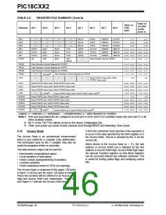
STATUS
TMR0H
TMR0L
T0CON
—
—
—
—
Indirect Data Memory Address Pointer 2 High Byte
---- 0000
xxxx xxxx
---x xxxx
0000 0000
xxxx xxxx
1111 1111
---- 0000
uuuu uuuu
---u uuuu
0000 0000
uuuu uuuu
1111 1111
Indirect Data Memory Address Pointer 2 Low Byte
—
—
—
N
OV
Z
DC
C
Timer0 register high byte
Timer0 register low byte
TMR0ON
T08BIT
T0CS
T0SE
PSA
T0PS2
T0PS1
T0PS0
Legend: x = unknown, u = unchanged, - = unimplemented, q = value depends on condition
Note 1: RA6 and associated bits are configured as port pins in RCIO and ECIO oscillator mode only and read ’0’ in all
other oscillator modes.
2: Bit 21 of the TBLPTRU allows access to the device configuration bits.
3: Other (non-power-up) resets include external reset through MCLR and Watchdog Timer Reset.
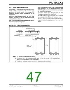
DS39026B-page 44
Preliminary
7/99 Microchip Technology Inc.

 MICROCHIP [ MICROCHIP ]