PIC18CXX2
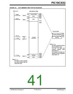
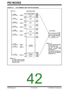
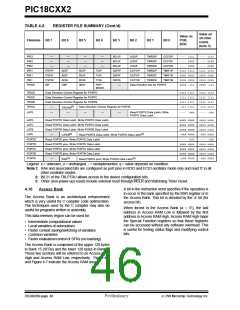
FIGURE 4-7: DATA MEMORY MAP FOR PIC18C252/452
BSR<3:0>
= 0000b
Data Memory Map
000h
07Fh
080h
0FFh
00h
Access RAM
GPR
Bank 0
FFh
00h
100h
= 0001b
= 0010b
GPR
GPR
Bank 1
Bank 2
Bank 3
1FFh
200h
FFh
00h
2FFh
300h
FFh
00h
= 0011b
= 0100b
= 0101b
GPR
FFh
3FFh
400h
Access Bank
Bank 4
Bank 5
GPR
GPR
4FFh
500h
00h
7Fh
80h
Access RAM low
00h
FFh
Access RAM high
FFh
5FFh
600h
(SFR’s)
When a = 0,
= 0110b
= 1110b
the BSR is ignored and the
Access Bank is used.
The first 128 bytes are
General Purpose RAM
(from Bank 0).
Bank 6
to
Bank 14
Unused
Read ’00h’
The second 128 bytes are
Special Function Registers
(from Bank 15).
EFFh
F00h
F7Fh
F80h
FFFh
00h
FFh
Unused
SFR
= 1111b
Bank 15
When a = 1,
the BSR is used to specify
the RAM location that the
instruction uses.
DS39026B-page 42
Preliminary
7/99 Microchip Technology Inc.

 MICROCHIP [ MICROCHIP ]