PIC18CXX2
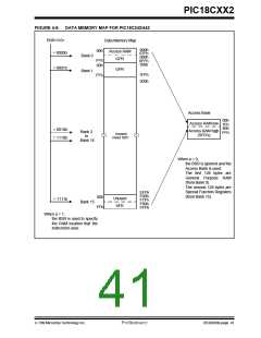
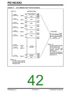
FIGURE 4-6: DATA MEMORY MAP FOR PIC18C242/442
BSR<3:0>
= 0000b
Data Memory Map
000h
07Fh
080h
0FFh
100h
00h
Access RAM
GPR
Bank 0
Bank 1
FFh
00h
= 0001b
GPR
1FFh
200h
FFh
Access Bank
00h
Access RAM low
7Fh
80h
= 0010b
= 1110b
Access RAM high
FFh
Bank 2
to
Bank 14
Unused
Read ’00h’
(SFR’s)
When a = 0,
the BSR is ignored and the
Access Bank is used.
The first 128 bytes are
General Purpose RAM
(from Bank 0).
The second 128 bytes are
Special Function Registers
(from Bank 15).
EFFh
F00h
F7Fh
F80h
FFFh
00h
FFh
Unused
SFR
= 1111b
Bank 15
When a = 1,
the BSR is used to specify
the RAM location that the
instruction uses.
7/99 Microchip Technology Inc.
Preliminary
DS39026B-page 41

 MICROCHIP [ MICROCHIP ]