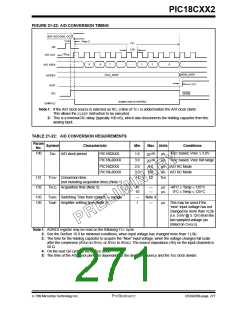
PIC18CXX2
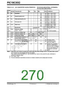
TABLE 21-21: A/D CONVERTER CHARACTERISTICS: PIC18CXX2 (INDUSTRIAL, EXTENDED)
PIC18LCXX2 (INDUSTRIAL)
Param
No.
Symbol Characteristic
Min
Typ
Max
Units Conditions
A01
NR
Resolution
—
—
—
—
10
TBD
bit VREF = VDD ≥ 3.0V
bit VREF = VDD < 3.0V
A03
A04
A05
A06
A10
EIL
Integral linearity error
Differential linearity error
Full scale error
Offset error
—
—
—
—
<±1
TBD
LSb VREF = VDD ≥ 3.0V
LSb VREF = VDD < 3.0V
EDL
EFS
EOFF
—
—
—
—
<±1
TBD
LSb VREF = VDD ≥ 3.0V
LSb VREF = VDD < 3.0V
—
—
—
—
<±1
TBD
LSb VREF = VDD ≥ 3.0V
LSb VREF = VDD < 3.0V
—
—
—
—
<±1
TBD
LSb VREF = VDD ≥ 3.0V
LSb VREF = VDD < 3.0V
guaranteed(3)
—
Monotonicity
—
VSS ≤ VAIN ≤ VREF
A20
A20A
A21
A22
A25
A30
VREF
Reference voltage
(VREFH - VREFL)
0V
3V
—
—
—
—
V
V
For 10-bit resolution
VREFH Reference voltage High
VREFL Reference voltage Low
AVSS
AVSS - 0.3V
AVSS - 0.3V
—
—
—
—
—
AVDD + 0.3V
AVDD
V
V
VAIN
ZAIN
Analog input voltage
VREF + 0.3V
10.0
V
Recommended impedance of
analog voltage source
kΩ
A40
A50
IAD
A/D conversion PIC18CXXX
—
—
180
90
—
—
µA Average current
current (VDD)
consumption when
A/D is on. (Note 1)
PIC18LCXXX
µA
IREF
VREF input current (Note 2)
10
—
1000
µA During VAIN acquisition.
Based on differential of
VHOLD to VAIN. To charge
CHOLD see Section 16.0.
During A/D conversion
µA cycle
—
—
10
Note 1: When A/D is off, it will not consume any current other than minor leakage current. The power-down current
spec includes any such leakage from the A/D module.
VREF current is from RA2/AN2/VREF- and RA3/AN3/VREF+ pins or AVDD and AVSS pins, whichever is
selected as reference input.
2: VSS ≤ VAIN ≤ VREF
3: The A/D conversion result either increases or remains constant as the analog input increases.
DS39026B-page 270
Preliminary
7/99 Microchip Technology Inc.

 MICROCHIP [ MICROCHIP ]